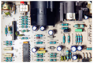
I don't know if you have found such a phenomenon, that is, most of PCB layers are designed as even layers, such as common 4 Layer PCB, 6 Layer PCB, etc. So why is that? As a matter of fact, even-layer PCB do have more advantages than odd-layer PCB.
Advantages Of Even Layer PCB
1. Low Cost
Due to the lack of a layer of dielectric and foil, the raw material cost of odd-layer PCB is slightly lower than that of even-layer PCB. However, the processing cost of odd-layer PCB is significantly higher than that of even-layer PCB. That’s to say, for odd-layer PCB, although the processing cost of the inner layer is the same, but the foil/core structure significantly increases the processing cost of the outer layer.
Odd-layer PCB need to add a non-standard laminate bonding process to the core structure process. Compared with the nuclear structure, the production efficiency of the factory that adds foil to the nuclear structure will decrease. Before lamination, the outer core requires additional processing, which obviously increases the risk of scratches and etching errors on the outer layer.
2. Balance The Structure & Avoid Bending
The vital reason why PCB layer isn’t designed as odd-layer is that odd-layer PCB is easy to bend. When the PCB is cooled after the multilayer circuit bonding process, when the core structure and the foil coating structure are cooled, different lamination tensions will cause the PCB to bend. As the thickness of the circuit board increases, the risk of bending the composite PCB with two different structures also increases. Therefore, the solution to eliminating circuit board bending is to use balanced delamination. Although a certain degree of bending PCB meets the specification requirements, the subsequent PCBA processing efficiency will be reduced, resulting in an increase in cost. As the assembly requires special equipment and craftsmanship, the placement accuracy of the parts is reduced, and the quality will be damaged.
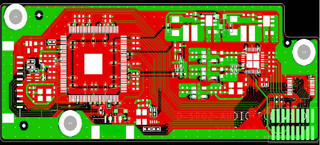
The changes are easier to understand: In the PCB technology process, 4 Layer PCB is better than the 3 Layer PCB in controlling, mainly in terms of symmetry; Exactly speaking, the warpage of 4 Layer PCB can be controlled below 0.7% (IPC 600 standard), but 3 Layer PCB whose size and warpage will exceed the standard, which will affect the reliability of SMT and the entire product. Thus, for ordinary PCB designers, do not design an odd layer board. Even if PCB is an odd layer function, which usually tends to design the counterfeit into an even layer. For example, 5 Layer PCB design is divided into 6 Layer , and the 7 Layer PCB design is divided into 8 Layer.
In the light of the above reasons, most of multi-layer PCB is often designed as even layers, and rarely used odd layers.
How Can We Balance Cascade & Reduce The Cost Of Odd-Layer PCB?
Speaking of an odd PCB layer appears in the PCB design, the following methods are able to balance the cascade, reduce the production cost of the PCB and avoid PCB bending.
1. Add An Extra Signal Layer & Make Use Of It
This method can be used if the power layer of the PCB is even and the signal layer is odd. Adding layers will not increase costs, instead, which is going to reduce delivery time and improve PCB quality.
2. Add An Additional Power Layer
If the power layer of PCB is odd and the signal layer is even, then adding an additional power layer will be helpful; And the easy way is to add a layer in the middle of the stack without changing other settings. First, arrange the odd layer on the PCB, then copy the middle layer and mark the remaining layers. This is similar to the electrical properties of foils applied in thickened layers.
3. Add A Blank Signal Layer Near The Center Of PCB
This method minimizes stacking imbalance and improves PCB quality. First, layout on the odd layers, then add blank signal layers, and mark the remaining layers. By the way, such method, add a blank signal layer near the center of PCB which is used in microwave circuits and mixed medium (different dielectric constant) circuits.