
Grande Electronics specializes in providing overall PCBA electronics manufacturing services, including one-stop services from upstream Electronic Components Procurement to PCB Manufacturing, PCB Assembly, SMT, DIP, PCBA Testing as well as finished box assembly. Now, Grande will introduce the defects & solutions of QFN and LGA voiding in SMT soldering;
1. Introduction
There are a great number of terrible impact of voiding, such as reliability issue, heat dissipation issue, various failures issue, customer complaints, etc. So do you want to solve the annoying voiding problem?
Causes Of Voiding In QFN Components
>Rapid growth, the bottom heat dissipation pad is too large, and the cavity is >25%
>Steel mesh design>Furnace temperature adjustment>Solder paste adjustment
>Another simple and convenient solution-one-how to apply soldering lugs to QFN and LGA components voiding?
2. Reasons Of QFN Voiding
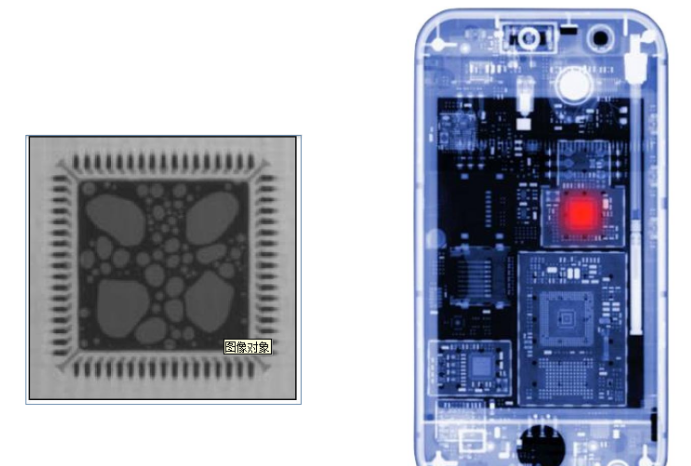
QFN Structure Diagram
>Four-side flat package without leads
>The grounding pad is under the component, usually its size is 4mm*4mm
>The ground pad is in direct contact with the solder paste
Solder Paste and Stencil
>The volume of flux in the solder paste occupies 50%. The more the amount of tin, the larger the amount of flux.
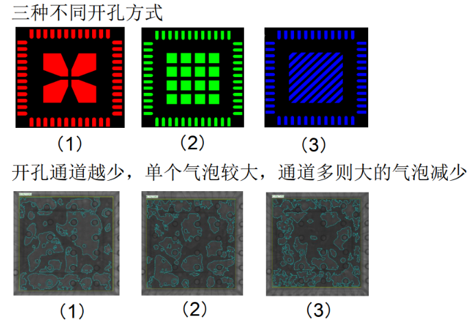
>For stencil openings, more air outlet channels are needed, but too many channels mean less tin.
Excessive Voidings Will Cause Short-Term Product Failure or Long-Term Reliability Risks
>The hazard of a single large cavity during PCBA assembly
>LED, automotive electronics, mobile phone products, and many industrial products are extremely sensitive to voiding and require to reduce the quantity of voiding.
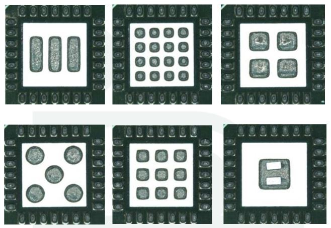
2.1 The Influence Of Stencil Design To Voiding
Through X-ray inspection, it is found that most of the time the shape of QFN voiding is only one or several larger voilding;
In the experiment, the size of the QFN ground pad is 4.1mm*4.1mm. In the stencil design, we use the following methods
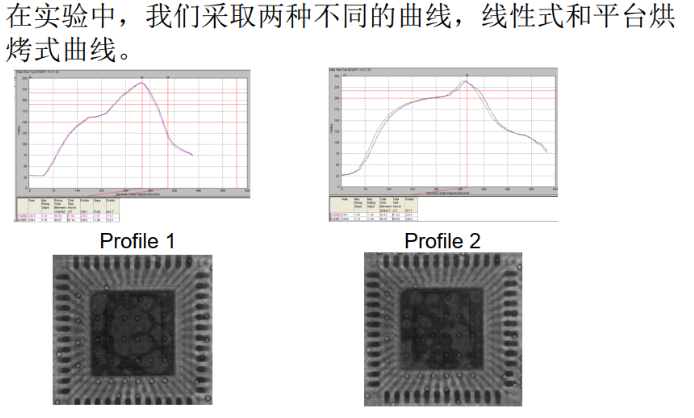
2.2 The Influence Of Furnace Temperature Design To Voiding
3.3 Solder Paste A djustment
Due to the flux is difficult to volatilize in the molten solder joints, so
-Appropriate high boiling point solvent
-Concern volatility of solvent
Increase the activity of flux
A better solderability which helps to squeeze out air in the flux.
3. Another Solution-Soldering Lug
What is a soldering lug?
>The same properties as solder paste, the same alloy of solder SnPb, SAC305, etc.
>Solid, different shapes, square, round, irregular shapes
>Volume can be accurately calculated
>Only need 1%~3% flux or no flux
Why need flux in soldering lug?
>Flux plating on the surface of the soldering pad is able to remove oxidation for QFN pad and PCB PAD so that helping soldering.
1%~3% Flux will not form large gassing and cause too large voiding.
4. How Can We Apply Solder Lugs To QFN Components?
The thickness of the solder lug
>In the experiment, the size of the grounding pad is 4.1mm*4.1mm, the size of the soldering pad is 3.67mm*3.67mm*0.05mm, and the surface is plated with 1% flux;
>Generally speaking, the size of the solder pad accounts for 80%-90% of the size of the pad;
Soldering / Stencil thickness-- 50~70%
In the experiment, the stencil is 4 mils thick, and the soldering lug thickness is 2 mils. On the QFN pad opening, the ground pad doesn’t need solder paste soldering, just open a 0.4mm round hole at each of the four corners to fix the solder lug.
5. How Can We Do SMT?
>Material tape loading, SMT machine automatic placement
>Or choose box, tray, or bulk, manual placement
SMT furnace temperature adjustment
>No need, go through the furnace with other components
>The same alloy, the same temperature
>Only 1%~3% flux, no requirement for gassing
Soldering Effect
> Compared with solder paste, 1% flux in the soldering lug not only reduces the proportion of flux, but also reduces the content of volatiles. ( PS: Due to the flux in the soldering lug is mainly solid)
>1% of flux can remove the oxidation of the pad surface and help form a good soldering.
>The voiding ratio is 3~6%, and the single largest voiding is about 0.7%.
6. What Is LGA Voiding?
LGA pads-58 round pads with a diameter of 2mm and 76 round pads with a diameter of 1.6mm, with vias on the pads. The voiding ratio is between 25%-45%.
Solution 1---Use solder lugs to reduce voiding to 6-14%
Solution 2---Indium10.1HF
Solder lug and solder paste compatibility issues
No-clean solder paste and no-clean flux are used in the experiment;
If the solder paste is water-washed, the surface of the solder sheet can be used without flux, but whether the soldering effect reaches the ideal value needs to be confirmed;
The solder paste only need to print the four corners of the QFN grounding pad, and the requirement for the amount of tin is as small as possible. It only serves as a fixed pad;
The size of the solder lug is generally 80% of the ground pad;
The thickness of the solder lugt is generally 50% to 70% of the thickness of the stencil solder paste printing;
The weight ratio of no-clean flux is generally 1.5%;
Need to consider no-clean flux compatibility;
Also pay attention to the pressure not to be too large when SMT, so as not to cause the solder lug squeezed and deformed, then no additional adjustment of the furnace temperature curve is required;
7.Conclusion
The influence of different solder pastes on the voiding of QFN is huge. The opening of stencil and the adjustment of the soldering furnace have certain help to reduce voiding.
>Various shapes of solder lug, with flux on the surface, very low flux residue after the furnace;
>It can be packaged with tape, SMT placement equipment can quickly and accurately mount;
> During reflow, no need to modify the furnace temperature;
>Very low void rate, whether it is a large pad or a small pad;
>In addition, when SMT can't provide sufficient amount of solder by printing solder paste alone, mounting solder can provide accurate and repeatable solder dosage, which is able to increase the amount of solder.


