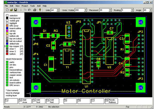
PCB design layout rules
1.Generally, all components should be arranged on the same side of the circuit board. Only the top layer components are too dense can some components with limited height and low heat generation, such as SMD resistors, SMD capacitors and SMD IC are goign to be placed on the lower layer.
2. On the premise of ensuring electrical performance, components should be placed on a grid and arranged parallel or perpendicular to each other consideringr neat and charming appearance. What’s more, components are not allowed to overlap; Components should be arranged compactly, and whose distribution should be even.
3. The minimum distance between the adjacent pad of different components on the circuit board should be over 1MM.
4. Not less than 2MM from the edge of the circuit board. The optimal shape of the circuit board is rectangular, and the aspect ratio is 3: 2 or 4: 3. However, if the surface area of the circuit board is larger than 200MM by 150MM, we should consider whether the circuit board can bear Mechanical strength or not.
PCB design layout tips
In the layout design of the PCB, the units of the circuit board should be analyzed, and the layout design should be performed according to the functions. When laying out all the components of the circuit, the following principles must be met:
1. Arrange the position of each functional circuit unit according to the flow of the circuit, make the layout convenient for signal circulation, and keep the signal in the same direction as possible.
2. Regard the core components of each functional unit as the center, then PCB layout around them. Furthermore, the components should be evenly, integrally and compactly arranged on the PCB to minimize and shorten the leads and connections between the components.
3. As for those circuits which are operating at high frequencies, the distribution parameters between components must be considered. In a word, the components should be arranged in parallel as much as possible, which looks not only gorgeous, but also be easy to install and mass production.
PCB design layout check
1. Whether the size of the circuit board and the drawing are in accordance with the processing size.
2. Whether the layout of the components is balanced, arranged neatly, or
all layout.
3. Whether there are conflicts at each layers. For example, are all the components, the frame, and the layer of silkscreen necessary?
4. Whether the commonly used components are convenient to use in practical. Such as switches, plug-in boards insertion device and components that will be replaced frequently.
5. Whether the distance between the thermal components and the heating components is reasonable.
6. Whether the heat dissipation is good.
7. Whether the problem of line interference need to be considered, etc.