Reference designators are an important way to identify components, but in real application they are not used consistently which can sometimes cause problems. This post will overview the basics of reference designator formats.
In general, reference designators are a letter followed by a number. Each location on a PCB will have a unique reference designator. While standardized, the letters sometimes vary. For instance, resistors use an “R” and capacitors use a “C.” Integrated circuits mostly use “U,” but “IC” is also used. By the standards, crystals and oscillators should be designated with a “Y,” but “X”, “Q” and “U” are also used, which can cause confusion. The confusion increases quite a bit when greater than ten of a certain type of part is used or when building a family panel, which are a lot of different designs in one PCB panel.
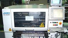
For instance, let’s say a PCB has 15 resistors. These could be designated as R1, R2, R3 through R15. But, someone else might designate them as R01, R02, R03 through R15. These two ways of designating the same parts is generally not a problem for a human being. But for a surface mount, pick and place robot, it can cause a problem because R1 and R01 are different parts to the robot. The best rule is to designate the components consistently. Assembly robots or systems interpret reference designators as text items, not numbers.
Let’s now consider a family panel. If one PCB designates C1 and C2 as a 10uf, 24V tantalum capacitor and another PCB designates C1` as a .01uf, 50V ceramic cap and C2 as a 220uf 24V metal can electrolytic cap, these inconsistent designations will confuse an automated surface mount machine assembling a family panel. (The different reference designators would be fine if you were to assemble the PCBs separately.)
One solution is to process your PCBs through the machine separately and not in family panels. Unfortunately, this is not always practical. Another solution is to designate the components of the PCBs consecutively. That is, PCB #1: R1, R2, R3, R4 and PCB #2: R5, R6, R7, R8. In essence you are treating the family panel is one complete large design. Of course, this approach can cause confusion down the road when rework is necessary.
One thing you should most certainly avoid is the odd/even reference designator (e.g., PCB#1: R1, R3, R7. PCB#2: R2, R4, R6, R8.) This would only be confusing. A better way to designate components would be: PCB#1: R101, R102, R103 and PCB#2: R201, R202, R203.
Welcome to Shenzhen Grande Electronic Co., Ltd.!


