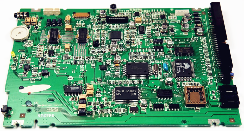
Grande Electronics specialized in providing all in one PCBA electronic manufacturing services, including PCB Layout, Components Procurement, PCB Fabrication, PCB Assembly, Functional Test, Final Box Build, etc as well as high-density circuit boards Design prototype service.
The Pros of high-density circuit board design Prototype:
1. The same product PCB design can reduce the number layers of support plate, increase density and reduce cost.
2. Increasing the routing density and using tiny-hole fine trace to increase the circuit capacity per unit area so that which can meet the assembly requirements of high-density contact components and facilitate the use of advanced structures.
3. The use of tiny-hole interconnection can shorten the contact distance, reduce signal reflection, and crosstalk between lines, and the components also have better electrical performance and signal accuracy.
4. The structure adopts a thinner dielectric thickness, and the potential inductance is relatively low.
5. The tiny-hole has a low aspect ratio, and the signal transmission reliability is higher than that of the general through-hole.
6. The micro-hole technology allows the carrier PCB design to shorten the distance between grounding and signal layers, thereby improving radio frequency/electromagnetic wave/electrostatic discharge (RFI/EMI/ESD) interference. The number of grounding wires can be increased to prevent components from being damaged by instantaneous discharge caused by static electricity accumulation.
7. Tiny-holes can increase the flexibility of circuit configuration and make circuit PCB design easier. Modern popular electronic products must not only have the characteristics of mobility and power saving, but also have no burden to wear, beautiful appearance, of course, the most important thing is the price is affordable and can be replaced with fashion.
High-Density Circuit Board Design Capabilities
The highest signal design rate: 10Gbps CML differential signal;
The highest PCB design layers: 40 layers;
Minimum line width: 2.4mil;
Minimum line spacing: 2.4mil;
Minimum BGA PIN spacing: 0.4mm;
Minimum mechanical hole diameter: 6mil;
Minimum laser drilling diameter: 4mil;
Maximum PIN number:; 63000+
Maximum number of components: 3600;
Maximum number of BGA: 48+.
High-Density Circuit Board Prototype Capability
1. The largest board: 310mm*410mm (SMT);
2. Maximum board thickness: 3mm;
3. Minimum board thickness: 0.5mm;
4. The smallest Chip package: 0201 package or package above 0.6mm*0.3mm;
5. The maximum weight of the mounted components: 150 grams;
6. Maximum part height: 25mm;
7. Maximum component size: 150mm*150mm;
8. Minimum lead part spacing: 0.3mm;
9. The smallest spherical part (BGA) spacing: 0.3mm;
10. The smallest spherical part (BGA) diameter: 0.3mm;
11. Maximum component placement accuracy (100QFP): 25um@IPC;
12. SMT capacity: 3 to 4 million points/day.
Four Reasons Why Choosing Grande To Do SMT
1. Strength Guarantee
▪ SMT factory: With imported SMT machines and multiple optical inspection equipment, which is able to produce 4 million points per day. Each process is equipped with QC personnel who will keep an eye on product quality.
▪ DIP production line: Two wave soldering machines and more than 10 employees who have worked for over three years. That’ s to say, these workers are highly skilled and can weld various SMT & DIP components.
2. Quality Assurance With High Cost Performance
▪ High-end equipment can paste precision special-shaped parts, BGA, QFN, 0201 package. It can also be soldered prototype pcba via SMT machine and placing bulk materials by hand.
▪ Both samples, small and large batches can be produced. And there is no SMT Machine starting cost.
3. Rich Electronic Products SMT Soldering Experience With Stable Delivery
▪ Accumulated services to thousands of electronics companies, involving SMT soldering services for various types of automotive equipment and industrial control motherboards. Furthermore, PCBA products are often exported to Europe and the United States, and the quality is able to be affirmed by new and regular customers.
4. Strong Maintenance Ability & Reliable After-Sales Service
▪ The maintenance engineers have sophisticated experience so that those defective boards caused by all kinds of smt soldering can be repaired. Meanwhile, ensuring the connectivity rate of each circuit board also make sense.
▪Order problems feedback will get response, solution and solved as soon as possible.