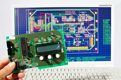
Grande Electronics is a PCB design company specializing in electronic product circuit board layout. It mainly undertakes multi-layer, high-density PCB layout and circuit board prototype business. Next, Grande will introduce the solution for impedance discontinuity in PCB Layout.
What Is Impedance?
To clarify a few concepts first, we often see impedance, characteristic impedance and instantaneous impedance. Strictly speaking, they are different, but they are always the same. They still comply with the basic definition of impedance:
a) The input impedance at the beginning of the transmission line is referred to as impedance;
b) The instantaneous impedance encountered by the signal at any time is called the instantaneous impedance;
c) If the transmission line has a constant instantaneous impedance, it is called the characteristic impedance of the transmission line.
The characteristic impedance describes the transient impedance that the signal receives when propagating along the transmission line, which is a major factor affecting the signal integrity in the transmission line circuit.
If there is no special instruction, characteristic impedance is generally used to collectively refer to transmission line impedance. The factors that affect the characteristic impedance are: dielectric constant, dielectric thickness, trace width, and copper foil thickness.
What Is Impedance Continuity?
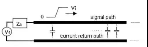
The impedance continuity is like water flows steadily in a uniform ditch, and suddenly the ditch turns and widens. Then the water will sway at the corners and cause water wave propagation, and which is the result of impedance mismatch.
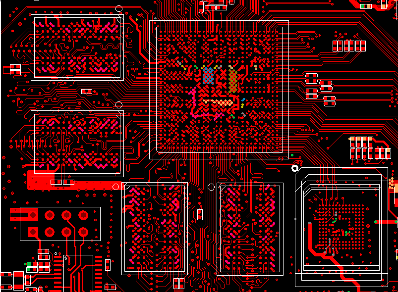
PCB Layout Impedance Discontinuity Solution
1. Tapered Line
Some RF components package is tiny, SMD pad width may be as small as 12 mils, but RF signal line width may reach 50 mils or more. Tapered lines must be used to prohibit line width mutations. The tapered line is shown in the figure, and the line of the transition part should not be too long.

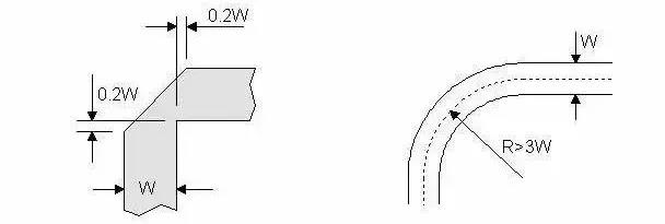
2. Corner
If the RF signal line runs at a right angle, the effective line width at the corner will increase, and the impedance will be discontinuous, causing signal reflection. In order to reduce the discontinuity, to deal with the corners, there are usually two methods: corner cutting and rounding. The radius of the arc angle should be large enough, generally speaking, to ensure: R>3W. As shown below.
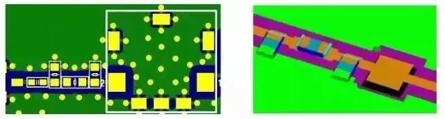
3. Large Pads
When there are large pads on the 50-ohm microstrip line, the large pads are equivalent to distributed capacitance, which destroys the characteristic impedance continuity of the microstrip line. Two methods can be taken to improve at the same time: Firstly, thickening the microstrip line dielectric; Secondly, hollowing out the ground plane under the pad, which will reduce the distributed capacitance of the pad. As shown below.
4. Vias
Vias are metal cylinders plated outside the through holes between the top and bottom layers of the circuit board. Signal vias connect transmission lines on different layers. The via stub is the unused part of the via. Via pads are annular spacers that connect the via to the top or internal transmission line. Isolation plates are annular gaps in each power or ground plane to prevent short circuits to the power and ground planes.
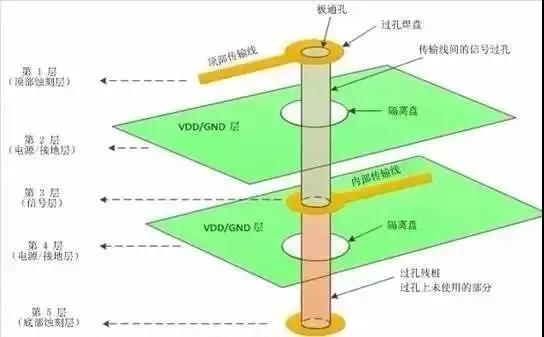
After rigorous physical theory derivation and approximate analysis, the equivalent circuit model of the via can be a grounded capacitor connected in series at both ends of an inductor, as shown in the figure below.
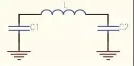
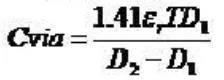
It can be seen from the equivalent circuit model that the via itself has parasitic capacitance to ground. Assuming that the diameter of the via anti-pad is D2, the diameter of the via pad is D1, the thickness of the PCB board is T, and the dielectric constant of the board substrate is ε, then the parasitic capacitance of the via is approximately:
The parasitic capacitance of the via can cause the signal rise time to be prolonged and the transmission speed to slow down, thereby degrading the signal quality. Similarly, vias also have parasitic inductance. In high-speed digital PCBs, the harm caused by parasitic inductance is often greater than parasitic capacitance.
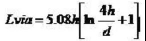
Its parasitic series inductance will weaken the contribution of the bypass capacitor, thereby weakening the filtering effect of the entire power system. Assume that L is the inductance of the via, h is the length of the via, and d is the diameter of the center hole. The approximate parasitic inductance of the via is similar to:
Vias are one of the important factors that cause impedance discontinuities on the RF channel. If the signal frequency is greater than 1 GHz, the impact of vias must be considered.
Common methods to reduce the discontinuity of via impedance include: adopting a diskless process, selecting an outlet method, and optimizing the anti-pad diameter. Optimizing the anti-pad diameter is a commonly used method to reduce impedance discontinuities. Since the characteristics of vias are related to structural dimensions such as aperture, pads, anti-pads, stacked structures, and wiring methods, it is recommended that HFSS and Optimetrics be used for optimization and simulation according to the specific circumstances during each design.
When using a parametric model, the modeling process is simple. During the review, PCB designers are required to provide corresponding simulation documents.
The diameter of the via, the diameter of the pad, the depth, and the anti-pad will bring changes, resulting in impedance discontinuity, reflection and insertion loss severity.
5. Through Hole Coaxial Connector
Similar to the via structure, the through-hole coaxial connector also has impedance discontinuities, so the solution is the same as that of the via. The common method to reduce the impedance discontinuity of the through-hole coaxial connector is also: adopt a diskless process, a suitable outlet method, and optimize the anti-pad diameter.