
Grande Electronics is not only specializing in PCB & PCBA, but also PCB Layout, especially in multi-layer and high-density electronic product PCB layout.
Speaking of starting PCB Layout, as you probably know, due to most of time is spent on circuit design and component selection so that in the PCB layout stage, which often occurs insufficient consideration issue due to lack of experience. That’s to say, if sufficient time and energy are not provided in the PCB layout stage, it may cause severe problems in PCB manufacturing or defects in PCB function when the design is transformed from the digital domain to the physical reality. So what is the key to layout a circuit board (PCB) that is real and reliable on both theory and physical form?
1. Fine-Tune Components Layout
The component placement of PCB layout is both science and art to some degree, requiring strategic consideration of the main components available on the circuit board. Although this process can be challenging, the way you place your electronic components will determine how easy your circuit board is to manufacture and how it meets your original design requirements.
Although there is a general sequence for component placement, such as placing connectors, printed circuit board mounting components, power circuits, precision circuits, and critical circuits in order. Apart from that, there are aslo a couple of specific guidelines that we should keep in mind, including:
Orientation-Ensure that similar components are positioned in the same direction, which will help achieve an efficient and error-free soldering process.
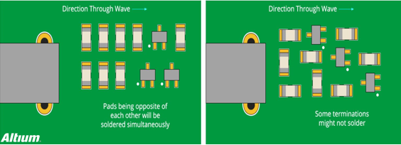
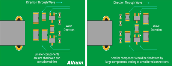
Layout-Avoid placing smaller components behind larger components, so that small components may be affected by the soldering of large components and cause mounting problems.
Organization-Place all surface mount (SMT) components on the same side of the circuit board, and place all through-hole (TH) components on the top of the circuit board to minimize assembly steps.
BTW, when using mixed technology components (through-hole and surface mount components), the PCBA manufacturer may require additional processes to assemble the circuit board, which will increase board overall cost finally.
2. Place Power, Ground & Signal Trace Properly
Once finished placing components on the board, we can place power, ground, and signal traces to ensure that the signals get a clean and trouble-free path. At this stage of the layout process, keep the following guidelines in mind:
Locate The Power & Ground Plane Layers
It is always recommended to place the power and ground plane layers inside the circuit board while maintaining symmetry and centering. This helps prevent circuit board ( PCB ) from bending, which is also related to the correct positioning of components. Regarding supplying power to the IC, it is recommended to use a common channel for each power supply to ensure a solid and stable trace width and avoid component-to-component daisy- style chain power connections.
Connect Signal Trace Routing
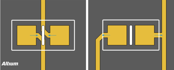
Next, connect the signal trace in the light of schematic. It is recommended to always take the shortest possible path and direct path between components. However, if the components need to be fixed and placed in the horizontal direction without deviation, which is recommended to route the traces basically horizontally where the components of the circuit board exit, and then perform vertical traces after exiting. In this way, as the solder moves during soldering, the components will be fixed in the horizontal direction. As shown in the upper part of the figure below. The signal routing method in the lower half of the figure below may cause component deflection as the solder flows during soldering.
Define Network Width
PCB Layout may require different networks, which will carry various currents, which will determine the required network width. Considering this basic requirement, it is recommended to provide 0.010’’ (10mil) width for low current analog and digital signals. When the trace current exceeds 0.3 amps, it should be widened. Here is a free trace width calculator to make this conversion process easy.
3. Isolate Circuit Effectively
We may have experienced how large voltage and current spikes in the power supply circuit can interfere with the low-voltage current control circuit. To minimize such interference issues, follow these guidelines:
Isolation-Ensure that each power supply is kept separate from power ground and control ground. If we must connect them together in the PCB, make sure it is as close as possible to the end of the power path.
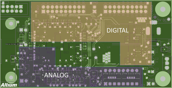
Placement-If we have placed a ground plane on the middle layer, make sure to place a small impedance path to reduce the risk of any power circuit interference and help protect the control signal. Or we can follow the same guidelines to keep your digital and analog grounds separate.
Coupling-In order to reduce capacitive coupling due to the placement of a large ground plane and traces above and below it, please try to cross the analog ground only through analog signal lines.
4. Solve Heat Issue
Have you ever caused the degradation of circuit performance or even the circuit board damage due to heat issue? Since heat dissipation is not considered, many problems have plagued many designers. Here are some guidelines to keep in mind to help solve heat issues:
Identify Troublesome Components
The first step is to start thinking about which components will dissipate the most heat on the board. This can be achieved by first finding the "thermal resistance" rating in the component's data sheet, and then transferring the generated heat in accordance with the recommended guidelines. Of course, radiators and cooling fans can be added to keep the component temperature down, and remember to keep key components away from any high heat sources.
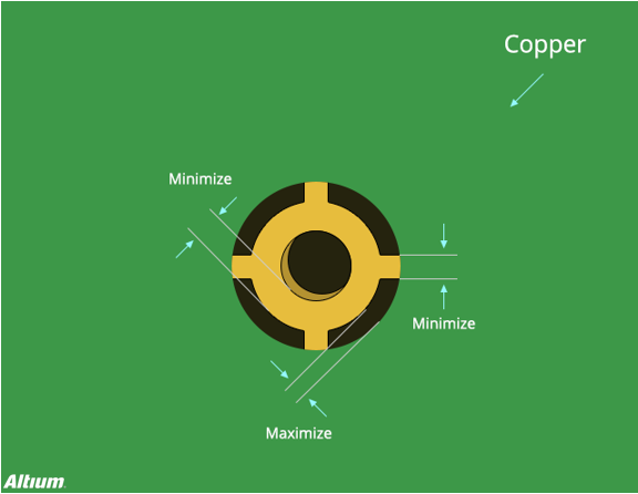
Add Thermal Relief Pads
The addition of thermal relief pads is extremely useful for producing manufacturable circuit boards. They are essential for wave soldering applications on high copper content components and multilayer circuit boards. Since it is difficult to maintain the process temperature, it is always recommended to use thermal relief pads on through-hole components to make the soldering process as simple as possible by slowing down the heat dissipation rate at the component pins.
As a general rule, always using thermal relief pads for any vias or vias that connect to the ground or power plane. In addition to the thermal relief pads, you can also add teardrops to the pad connection line to provide additional copper/metal support. This will help reduce mechanical and thermal stress.
Thermal Relief Pads Wiki
Engineers responsible for Process or SMT technology in many factories often encounter solder empty, de-wetting, or cold solder on circuit board components. For non-soldering defects, no matter how the process conditions are changed or the reflow furnace temperature is adjusted, there is a certain ratio of non-soldering failure. What happened?
Leaving aside the problem of component and circuit board oxidation, it is found that a large part of this type of poor soldering actually comes from the lack of good PCB layout, and the most common one is the soldering of certain components. The pins are connected to a large area of copper, which causes poor soldering of the solder pins of these components after reflow soldering. Besides, some manual soldered components may also cause false soldering or oversoldering problems due to similar situations, and some of them component is even broken due to heat up for a long time.
Generally, a large area of copper foil is often laid on PCB during layout to serve as power supply (Vcc, Vdd or Vss) and ground (GND, Ground). These large-area copper foils are generally directly connected to the pins of some control circuits (IC) and electronic components.
Unfortunately, if we want to heat these large areas of copper foil to the temperature of melting tin, which usually takes more time than a separate solder pad (that is, the heating will be slower), and the heat dissipation is faster. When one end of such a large area of copper foil wiring is connected to small components such as small resistors and capacitors, but the other end is not, soldering problems are likely to occur due to inconsistent tin melting and solidification time; If the temperature profile of reflow soldering is changed, the adjustment is not good and the preheating time is insufficient, the solder feet of these components connected to a large piece of copper foil are likely to cause the problem of virtual soldering because they cannot reach the melting temperature.
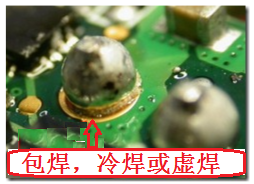
During manual soldering, the solder pins of these components connected to a large piece of copper foil will dissipate too quickly and cannot be soldered within the specified time. The most common undesirable phenomena are package soldering and virtual soldering. The solder is only soldered to the solder pins of the component and not connected to the pad of the circuit board. From the appearance, the entire solder joint will form a spherical shape; Moreover, the operator constantly increases the temperature of the soldering iron in order to solder the solder pins to the circuit board, or heats them for too long, causing the components exceeded the heat-resistant temperature. Damaged without knowing it. As shown below.
The most common undesirable phenomena are package soldering and virtual soldering. The solder is only soldered to the solder pins of the component and not connected to the pad of the circuit board. From the appearance, the entire solder joint will form a spherical shape; What’s more, the operator constantly increases the temperature of the soldering iron in order to solder the solder pins to the circuit board, or heats them for too long, causing the components to exceed the heat-resistant temperature. Damaged without knowing it.
Now that the problem is known, there can be a solution. Generally, we will require the so-called Thermal Relief Pad Design to solve this type of soldering problem caused by the solder pins of the large copper foil connecting components. As shown in the figure below, the trace on the left does not use thermal relief pad, while the trace on the right has been connected with thermal relief pad. It can be seen that the contact area between the pad and the large copper foil is only a few small lines. In this way, the temperature loss on the solder pad can be greatly restricted, and a better soldering effect can be achieved.
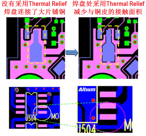
The trace on the left does not use thermal relief pad, while the trace on the right has already adopted the thermal relief pad connection method. It can be seen that the contact area between the pad and the large copper foil is only a few small traces, which can greatly limit the loss of temperature on the solder pads to achieve better soldering results.
5. Cross-check PCB Layout
When you hum and hum all the parts together for manufacturing, it is easy to find the problem at the end of the design project and become overwhelmed. Therefore, double- and triple-checking your design work at this stage may mean the success or failure of manufacturing.
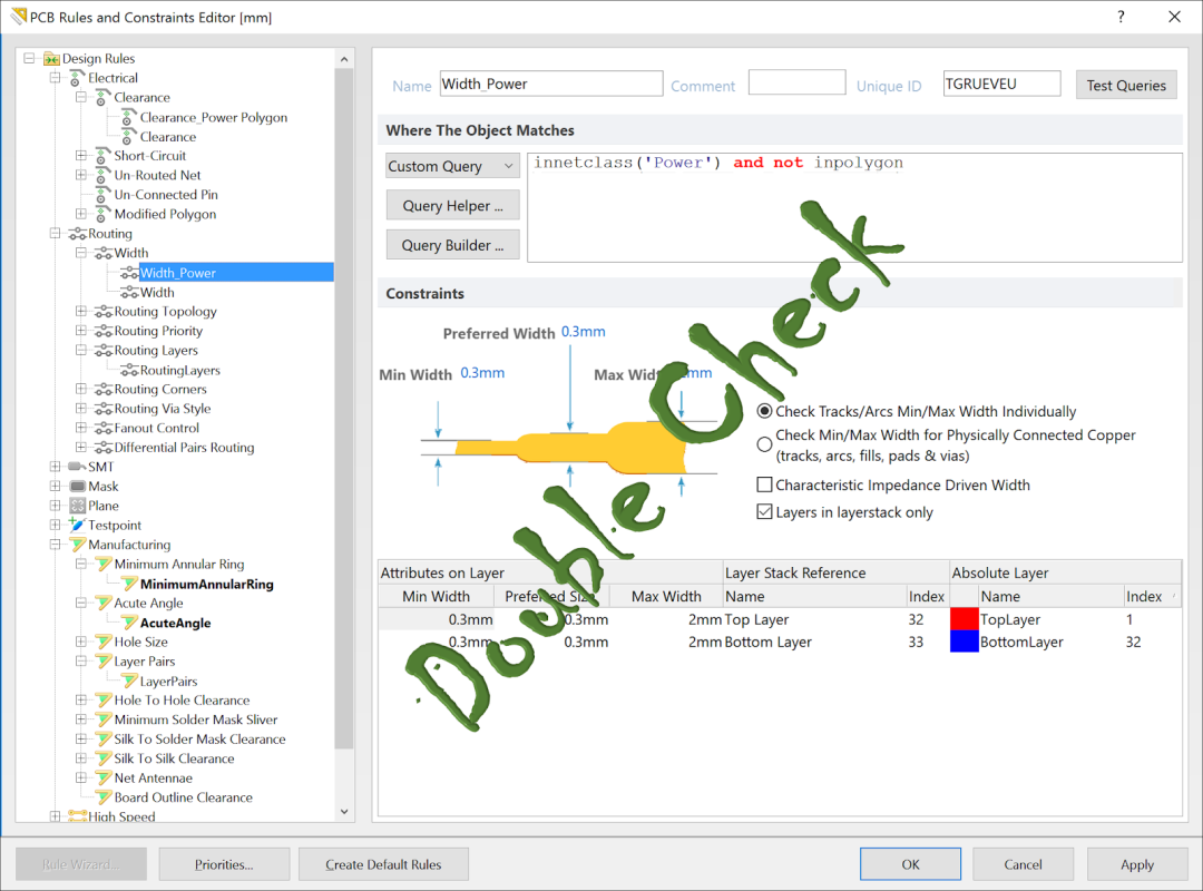
To help complete the quality control process, we always recommend that you start with Electrical Rule Check (ERC) and Design Rule Check (DRC) to verify that your design fully meets all the rules and constraints. Using these two systems, you can easily check gap widths, line widths, common manufacturing settings, high-speed requirements and short circuits.
When your ERC and DRC produce error-free results, it is recommended that you check the wiring of each signal, from the schematic to the PCB, and check one signal line at a time to make sure that you have not missed any information. In addition, use the detection and shielding functions of your design tool to ensure that your PCB layout materials match your schematic.
Conclusion
When you have this-the top 5 PCB Layout guidelines that our PCB designers all need to know. By following these suggestions, you will soon be able to design powerful and manufacturable circuit boards handily with real quality Printed circuit board.


