
Grande Electronics is a circuit board manufacturer specializing in the manufacture of printed circuit boards, focusing on single, double-sided and multilayer circuit boards for 20+ years. That’s to say, we are able to provide multi-layer PCB prototype and small batch production services such as impedance boards, HDI boards, etc.
Here is the introduction of Commonly Used Board Material:
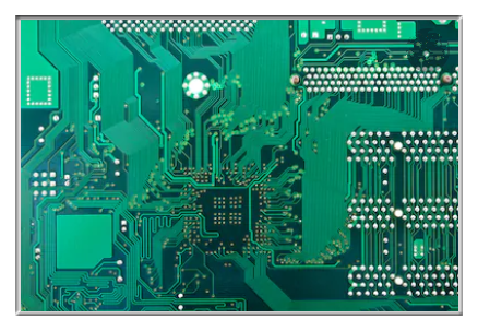
1. FR-4
FR-4 is an epoxy board with high mechanical and dielectric properties, good heat resistance and moisture resistance, and good mechanical processing.
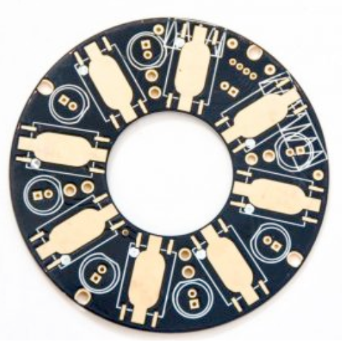
2. Aluminum Substrate
The aluminum substrate is a metal-based copper clad laminate with good heat dissipation function. Generally, a single panel is composed of a three-layer structure, which is a circuit layer (copper foil), an insulating layer and a metal base layer. Aluminum substrates are often used in LED lighting products. There are two sides, the white side is for soldering the LED pins, and the other side is the natural color of aluminum. Generally, the thermal conductive paste will be applied to contact the thermal conductive part.
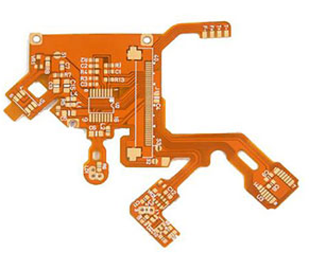
3. FPC Board
FPC board is a highly reliable and excellent flexible printed circuit board made of polyimide or polyester film. It has the characteristics of high wiring density, light weight, thin thickness and good bendability. Used in high-end products such as mobile phones and hard drives.
According to different product uses, the choice of PCBA substrate will be different. Generally, the higher-end product, the more advanced PCBA substrate used and the more expensive.
Grande’s PCB Manufacturing Capacity
PCB Layers: 2-40 layer;
PCB Thickness: 0.2-7.0mm;
Maximum Copper Thickness: 7oz;
Finished Product Size: 650*1100mm;
Minimum Line Width/Spacing: 3/3mil;
Maximum Board Thickness Aperture Ratio: 12:1;
Minimum Mechanical Drilling Diameter: 6mil;
Distance Between Via to Conductor: 3.5mil;
Impedance Tolerance (Ω): ±5%(<50), ±10%(≥50)
Surface Treatment: OSP, ENIG, HASL, Gold Finger, etc.;
Board Material: FR-4, High TG, Halogen-Free, High Frequency (Rogers, Isola...), CEM, etc.


