Shenzhen Grande Electronic Linkedin Page
Shenzhen Grande Electronic Co., Ltd logo
E-mail us for a Quote:
sales88@greattong.com
Call us now:
+86-755-83261869

Technical Article


Why do Pads lost and Pads deformation occur in PADS (PCB Design Software) ?

Time:2019-12-10 16:12:10 Click:

At present, most high-speed PCBs are designed via Cadence, PADS software and Altium Designer (AD). However, Companies that designed mobile phones in the early years are basically used to PADS.


Why do Pads lost and Pads deformation occur in PADS (PCB Design Software)?


1.Pads lost


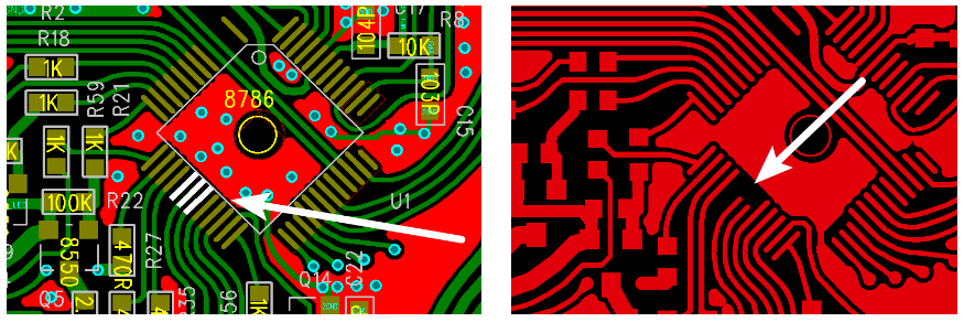
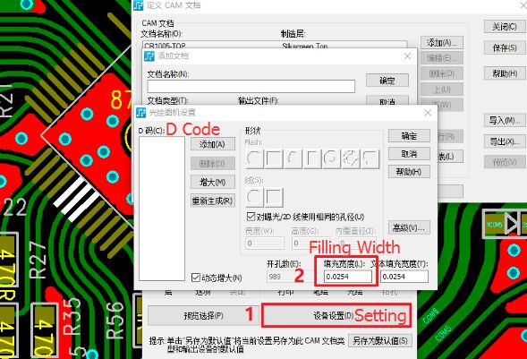
Reason:In PADS, beveled pads need to be filled when outputting Gerber. If the filled line is larger than the pad width, pad loss will occur.


Solution: Reducing the Fill Line Width when outputting light drawing.


2. Pads deformation


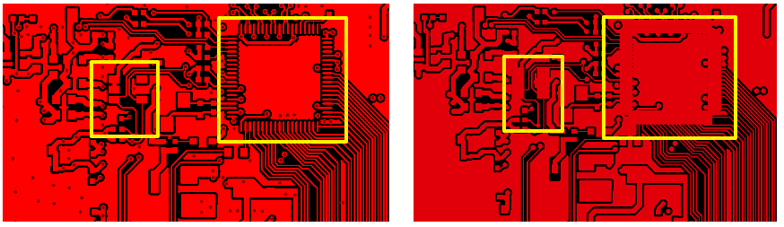
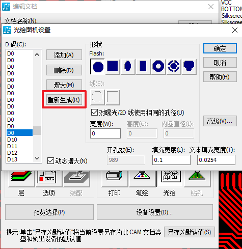
Reason: D code of the output Gerber is disordered.

Solution: Regenerating the D code table.


Previous:PCB design layout rules and techniques

Next:What are the difficulties in making multi-layer PCB?


Request an Official Quote

Questions

E-MAIL

File Upload

Upload a list of files

    Please upload your Gerber files and BOM. You can upload an unlimited number of files as long as the total size of all files does not exceed 20 MB. To ensure you receive your official quote in less than 24 hours, please include the quantity of circuit boards for which you would like a quote.

    If you require that we sign a Non-Disclosure Agreement (NDA), please send it to us prior to sending your files and we will be happy to accommodate.

     
    Home About Us Services Quality Pb-Free News Contact Us


    Copyright ® 2017,Shenzhen Grande Electronic Co., Ltd. All Rights Reserved. English 中文站 Sitemap