
SMTAssembly Solder Beads Defect Explanation
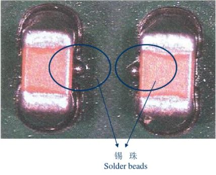
SMT Assembly solder beads defects not only affect the appearance but also cause bridging defects. Simply speaking, solder beads can be divided into two categories: One type appears on one side of the SMD component, often in the shape of an independent large ball (see Figure 1 below); The other type appears around the IC pins and which is in the shape of scattered beads.
Picture: Solder beads are located on the waist side of the component
Analysis of the Causes of Solder Beads Defect in SMT Assembly
Factor A: The temperature curve is incorrect▼
The reflow curve can be divided into 4 sections: Preheating, heat preservation, reflow and cooling. The purpose of preheating and heat preservation is to increase the surface temperature of the PCB to 150°C within 60-90s and keep it warm for about 90s so that it not only reduces the thermal shock of PCB and components, but also ensures that the solvent of the solder paste can be partially volatilized. Avoid splashing caused by too much solvent during reflow soldering, causing the solder paste to rush out of the pad and form tin beads.
Solution
The factory should pay attention to the heating rate and adopt moderate preheating to make the solvent fully volatilize
Factor B:The quality of solder paste▼
①The metal content in the solder paste is usually (90±0.5)℅. Too low metal content will cause too much flux composition, and too much flux will cause flying beads due to the fact that it is not easy to volatilize during the preheating stage;
②The increase of water vapor and oxygen content in the solder paste will also cause flying beads. Since solder paste is usually refrigerated, when it is taken out of the refrigerator, if it is not fully warmed to thaw and stirred evenly, water vapor will enter; in addition, the lid of the solder paste bottle must be tightly closed after using every single time. If it is not tightly closed in time, which will definitely cause the entry of water vapor;
③After the solder paste printed on the stencil is completed, the remaining part should be treated separately. If it is put back in the original bottle, the solder paste in the bottle will deteriorate and tin beads will also be produced;
Solution
The factory is required to choose high-quality solder paste and pay attention to the storage and use requirements of the solder paste.

Other factors include ▼
①The printing is too thick, and the excess solder paste overflows after the component pressed down;
②The pressure of the patch is too high, and the downward pressure will cause the solder paste to collapse onto the solder mask;
③The shape of the pad opening is not good, and no anti-tin bead treatment has been done;
④The activity of the solder paste is not good, it dries too fast, or there are too many small tin powders;
⑤The printing is offset, so that part of the solder paste is stained on the PCB;
⑥The scraper speed is too fast, causing bad edge collapse, and solder balls after reflow.


