
What’s The Cracking Solution Of SMD Components?
In SMT processing and assembly production, SMD Components are terribly common in MLCC. The cracking failure of MLCC is mainly caused by stress, including thermal stress and mechanical stress, that is, the cracking phenomenon of MLCC devices caused by thermal stress.
Reasons Of SMD Components Cracking
1. For MLCC capacitors whose structure is made by stacking multilayer ceramic capacitors, which means their structure is weak, low in strength, and has extremely strong heat resistance and mechanical impact, which is especially obvious in wave soldering;
2. During the SMT placement process, the suction and release height of the Z-axis of the placement machine, especially some placement machines that do not have the Z-axis soft landing function, the absorption height depends on the thickness of the SMD components instead of the pressure sensor, so that Tolerances in component thickness is easy to cause cracks;
3. After soldering, if there is warping stress on the PCB, it’s like a walk in the park to lead the components to crack.
4. PCB stress during splicing can also damage components.
5. The mechanical stress during the ICT test caused the device to rupture.
6. The stress during assembly will cause damage to the MLCC around the fastening screw.
Solutions
1. Adjusting the welding process curve carefully, especially pay attention to the heating speed should not be too fast;
2. During the placement, do ensure proper placement of the machine pressure, especially for thick plates and metal substrates, as well as ceramic substrates to install MLCC and other brittle components;
3. Pay attention to the placement method and shape of the cutter;
4. The warpage of the PCB, especially the warpage after soldering, should be specially corrected to prevent the stress caused by the large deformation from affecting the components;
5. During PCB design, avoiding high stress areas of MLCC and othercomponents.
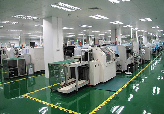
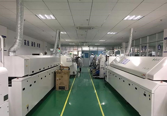
Grande SMT Processing Capability
1. The largest board: 310mm*410mm (SMT);
2. Maximum board thickness: 3mm;
3. Minimum board thickness: 0.5mm;
4. The minimum chip components: package 0201 or over 0.6mm*0.3mm;
5. Maximum weight of mounted components: 150g;
6. Maximum components height: 25mm;
7. Maximum components size: 150mm*150mm;
8. Minimum lead components gap: 0.3mm;
9. The minimum ball grid array (BGA) gap: 0.3mm;
10. The minimum ball grid array (BGA) diameter: 0.3mm;
11. Maximum component placement accuracy (100QFP): 25um@IPC;
12. Mounting capacity: 3 to 4 million points/day.
PCBA Production Flow
1. Customer Inquiries PCBA
Customer inquires PCBA and put forward specific requirements according to their actual needs. The PCBA Manufacturer will evaluate its own capabilities to see if it can complete the order. If the manufacturer determines that it can complete the order within the expected time, then the two parties will negotiate to determine the production details.
2. Customers Provides Production Files
Once the customer decides to place an order, he provides a series of files and lists to the PCBA manufacturer, such as the PCB Gerber file, coordinate files, and BOM lists required for production, which are all necessary.
3. Purchase Raw Materials
PCBA manufacturer purchases relevant raw materials from appointed suppliers according to the files provided by customers.
4. Incoming Material Inspection
Before PCBA production, all received raw materials are subjected to strict quality inspection to ensure that they are qualified and put into production.
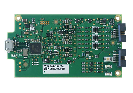
5. PCBA Production
During PCBA Assembly, in order to ensure production quality, whether it is SMD or solder production, PCBA manufacturers need to strictly control the furnace temperature.
6. PCBA Test
The PCBA manufacturer conducts strict product testing, and the PCBA that pass the test are delivered to the customer.
7. Packaging & After-Sale Service
As long as PCBA Assembly is completed, the product will be packaged and then delivered to the customer so that they are able to complete the entire PCBA work, including Box Build.


