Shenzhen Grande Electronic Linkedin Page
Shenzhen Grande Electronic Co., Ltd logo
E-mail us for a Quote:
sales88@greattong.com
Call us now:
+86-755-83261869

Technical Article


Why do we make cutouts and slots in the PCB board?

Time:2019-07-25 15:58:03 Click:

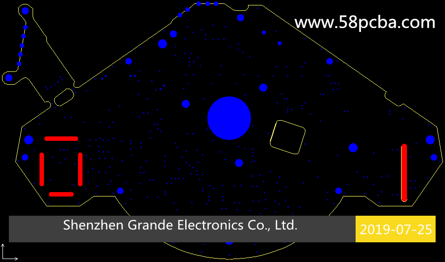
There are mainly three reasons why we make cutouts and slots in the PCB:


1. Structure and installation requirements;

2. To prevent the high-voltage components and near the low-voltage components on the PCB from being fired;

3. Adding the thermal pad by slotting, then it doesn’t need to consider electrical Safety requirements of electrical gap.


BTW, PCB slot design, whose processing of PCB file design is generally using Keep-Out layer or Mechanical layer.


Previous:Do ESD damaged PCBs ever look burnt?

Next:How do you solder electronic components?


Request an Official Quote

Questions

E-MAIL

File Upload

Upload a list of files

    Please upload your Gerber files and BOM. You can upload an unlimited number of files as long as the total size of all files does not exceed 20 MB. To ensure you receive your official quote in less than 24 hours, please include the quantity of circuit boards for which you would like a quote.

    If you require that we sign a Non-Disclosure Agreement (NDA), please send it to us prior to sending your files and we will be happy to accommodate.

     
    Home About Us Services Quality Pb-Free News Contact Us


    Copyright ® 2017,Shenzhen Grande Electronic Co., Ltd. All Rights Reserved. English 中文站 Sitemap