
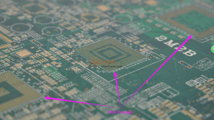
BGA means Ball Grid Array, which is a special type of SMD chip package;
So why is it called BGA? In fact, under the bottom of the package, all pins look like spherality and array as a grid pattern.
High-quality and Low-cost
PCB Manufacturing Services
![]() 1 to 30 Layers
1 to 30 Layers ![]() 100% Electrical Testing
100% Electrical Testing
![]() FR-4/Rogers/Teflon
FR-4/Rogers/Teflon ![]() Controlled Impedance
Controlled Impedance
Technical ArticleHow can we identify the BGA area of PCB?Time:2019-05-10 14:35:33 Click:
BGA means Ball Grid Array, which is a special type of SMD chip package; So why is it called BGA? In fact, under the bottom of the package, all pins look like spherality and array as a grid pattern.
Related articles:
Previous:How can I store my electronic components? Next:Is baking a graphics card in my oven dangerous? |
NewsOur Facilities |


