Shenzhen Grande Electronic Linkedin Page
Shenzhen Grande Electronic Co., Ltd logo
E-mail us for a Quote:
sales88@greattong.com
Call us now:
+86-755-83261869

Technical Article


What is a "buried via" on an electronics PCB?

Time:2018-11-09 09:39:13 Click:

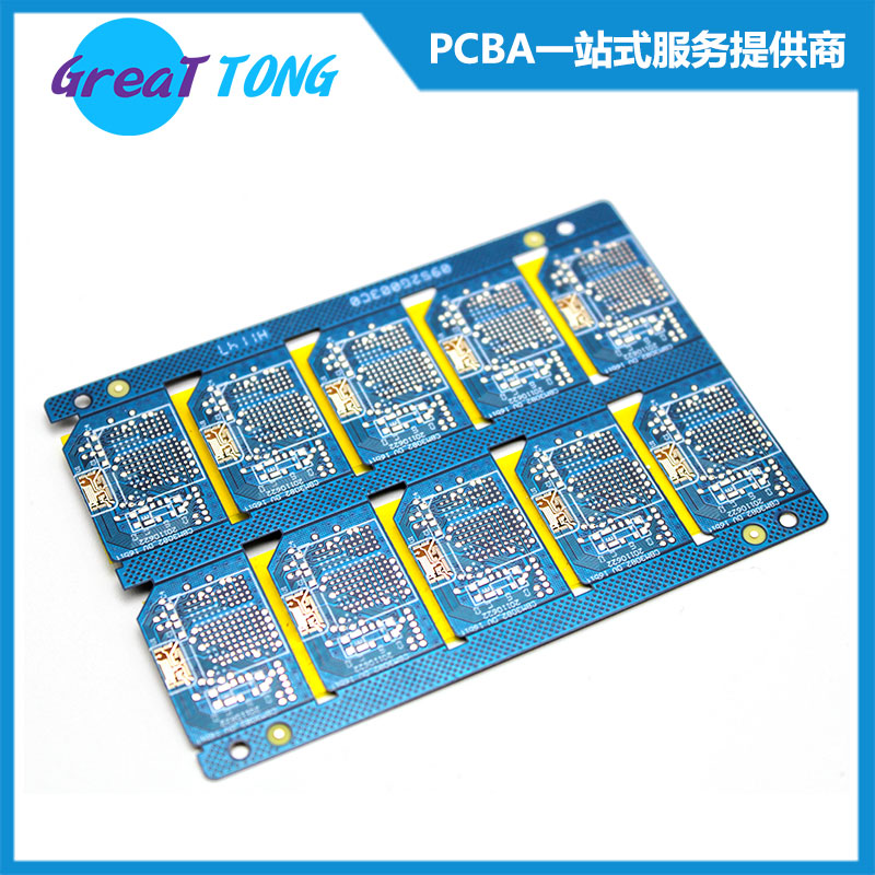
A buried Via means pass through the hole between inner layers of the PCB,

instead of the top and bottom layers, which is used to connect the signals of inner layers.


Application:


it’s widely used in the High density and high speed of PCB design, such as mobile phones and PAD board.


Function:


1)To reduce the rate of signal interference;

2)To maintain the continuity of transmission line about characteristic impedance;

3)To save the routing space.


However, the question is: the cost of buried via is not cheaper actually, which still need to be solved with the aid of the development of drilling technology.


Previous:Why are vias bad for high-frequency PCBs (Printed Circuit Boards)?

Next:How does a PCB assembly process work?


Request an Official Quote

Questions

E-MAIL

File Upload

Upload a list of files

    Please upload your Gerber files and BOM. You can upload an unlimited number of files as long as the total size of all files does not exceed 20 MB. To ensure you receive your official quote in less than 24 hours, please include the quantity of circuit boards for which you would like a quote.

    If you require that we sign a Non-Disclosure Agreement (NDA), please send it to us prior to sending your files and we will be happy to accommodate.

     
    Home About Us Services Quality Pb-Free News Contact Us


    Copyright ® 2017,Shenzhen Grande Electronic Co., Ltd. All Rights Reserved. English 中文站 Sitemap