After the reliability test of Turn-key Assembly , the component high resistance value is abnormal.
The computer simulates the element on the plate stress, which match normal but cannot pass practical measure of the PCBA. Is the element and the plate matching question? Or is there not enough tolerance to encapsulate tin balls? After reliability verification, the experimental results show that the failure point of high resistance value anomaly should be found.
How can we find the failure point?
Shenzhen Grande will share a case in which (WLCSP) is encapsulated in wafer size and the reliability of the upper plate is verified. This case is also a fairly common failure form for ICS with tin balls as encapsulation.
The so-called WLCSP wafer size package, full name wafer level chip scale packaging, means that the size of the package is equal to that of the original grain after the whole wafer level packaging process is finished and then cut, and the size of the package after cutting is equal to the original grain size. Subsequently, using the redistributed layer (RDL), I / O can be pulled out of the array tin sphere to connect with the PCB directly.
Due to the lightweight and short demand, WLCSP becomes the mainstream of encapsulation, and the wafer level packages such as fan-in, fan-out and info are derived under the concept of WLCSP . However, after reliability verification, common failure modes, such as tin ball interface, poor tin eating and post-plate stress matching, are common in this kind of packaging.
So, when it comes to identifying components in the form of WLCSP, at the point of failure after reliability verification, it's even more important to be aware of whether there is stress at the right point of the tool. Instead of destroying the killing site, it is harder to identify the cause of the failure.
How can we choose a failure analysis tool?
In the following case, Shenzhen Grande proposes three steps to tell you how to choose a failure analysis tool. In particular, at what point, the killing scene can be cleared, fast failure point defect no hiding, easy to find the true cause of failure.
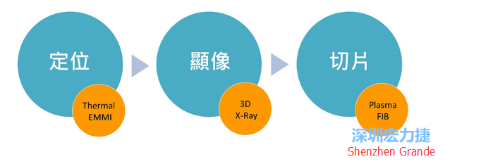
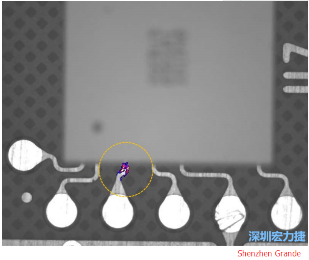
Step 1: Positioning
Aiming at the WLCSP element with high resistance after reliability test, the phase difference of thermal radiation conduction at the thermal EMMI fault point is used to locate the failure position, which is located in the solder ball.
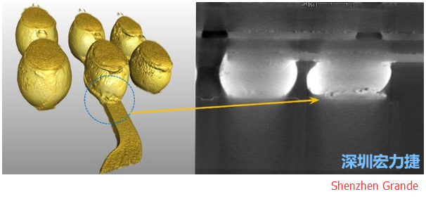
Step 2: Imaging
Then, in order not to destroy the "original failure scene", 3D X-ray was used to visualize stereoscopic (bottom left) and sectional (bottom right) images, and it was found that the solder ball was damaged.
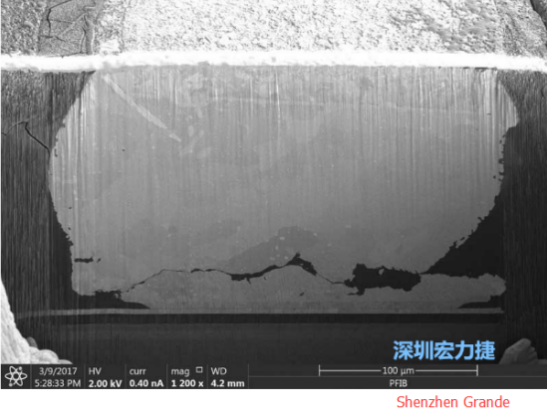
Step 3: Slicing
When the relative position of defect has been confirmed, the "original failure scene" can be removed at this time, and the failure section is cut out and the true cause is analyzed by using the low stress plasma fib tool. The original solder ball crack condition is found, which leads to the abnormal high resistance value of the component and the failure.