
1. Significance of good heat dissipation
As we all know, MID and VR devices are one of electronic devices. Except for useful work, most of the electrical energy consumed during work is converted into heat and emitted. The heat generated by the electronic equipment causes the internal temperature to rise rapidly. If the heat is not dissipated in time, the equipment will continue to heat up, and the device will fail due to overheating, resulting in a decrease in the reliability of the modified product. At the source end of electronic design, we need to fully consider heat dissipation, which is particularly important for PCB design to plan for making a good heat dissipation design.
2. The factors causing PCB board to heat up
The direct cause of PCB temperature rising that is due to the existence of circuit power consumption devices, which are generally caused by the following factors:
>The device selection is unreasonable and the power consumption is too large;
> The heat sink is not installed, resulting in abnormal heat conduction;
> The PCB is locally unreasonable, causing local or global temperature rise;
> PCB design, routing and heat dissipation design is unreasonable, causing heat concentration.
3. Thermal design PCB design planning
In view of common heat dissipation factors, when we plan the thermal design of PCB design, we propose some common solutions for this factor:
>Components selection
When selecting a model, the component with low power consumption is preferred under the premise that the same function can be realized. Meanwhile, this is also a cost consideration.
> Components layout
Before layout, we should start with the heat dissipation module from the Schematic, such as the common PMU module, DCDC module and some unit main control chips with relatively large heat dissipation, as shown in Figure 1. In the layout, we generally place these modules with large heat dissipation in blocks, and separate the non-severe heat dissipation modules with a distance of 3-5mm.
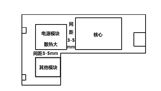
Figure 1 Distribution of PCB heat dissipation layout
At the same time, if conditions permit, heat sinks can be added to the main control chip with severe heat dissipation, as shown in Figure 2.
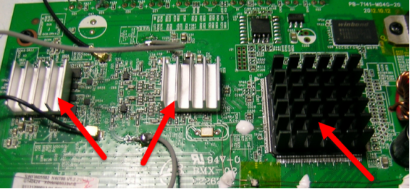
Figure 2 Increase the heat sink to enhance the heat dissipation method
3. Treatment of heat dissipation in PCB routing
PCB good copper wiring is also an important way to strengthen heat dissipation:
1) Add open vias to the heat dissipation pad of the chip, as shown in Figure 3, allowing the heat dissipated by the chip to be introduced into a large area of the same surface to disperse heat through the vias on the heat dissipation pad to achieve the purpose of heat dissipation.
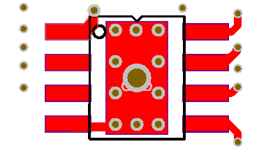
Figure 3 Adding a windowed via on the thermal pad
2) On the basis of perforating the heat dissipation pad, we will increase the heat dissipation area as much as possible. We can add copper leakage on the front and back impedance layers at the same time, and add heat dissipation vias at the same time.
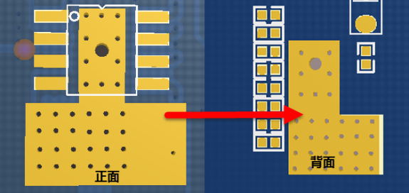
Figure 4 Open windows on the front and back to increase the heat dissipation area
The analysis of the above factors from PCB is an effective way to solve the temperature rise of the printed circuit board. These factors are often related and dependent on each other in a product and system. Most of the factors should be analyzed according to the actual situation, and only for a specific actual situation can solve the problem more correctly and reduce the temperature rise.


