At present, there are two kinds of lead processing technology in PCBA, which can be selected according to customer requirements, including HASL and HAL processing technology. However, there are plenty of customers who don’t really understand the difference between them. The only point most of customers know that is HASL processing is more expensive, while HAL processing is cheaper. The solder used in HASL processing is not 100% lead-free, but compared to Leaded solder contains lower lead elements.
The difference between HASL and HAL Processing
1. Cost
In the HASL processing process, some auxiliary materials are required for soldering due to the characteristics of the solder itself, and the use of HASL solder paste in reflow soldering increases the cost of using HASL solder paste by 2 times. At the same time, tin wire and tin bars that also need to be used to increase the processing cost by at least 2 times, so that the cost of HASL processing is higher;
2. Robustness
The melting point of the lead-free solder used in the HASL processing is 217℃, and the melting point of the HAL solder is only 183℃. Just because the melting point of the HAL solder is lower, which is the very reason why cause less thermal damage to electronic components. Besides, HAL processing also have other pros, such as the solder joints are brighter, the strength is harder, and the quality is better;
3. Reliability
The lead element contained in lead solder is harmful to the human body, and long-term exposure has a greater impact on human health. At the same time, HASL processing technology is widely used in the international market, which is also a kind of protection for the environment. After all, people have realized the harm caused by the increasingly serious environmental pollution.
In the electronic assembly or PCBA, the relevant electronic processing factories can make process selection based on the above, but can not pursue the advantages of HASL technology and reject the HAL technology.
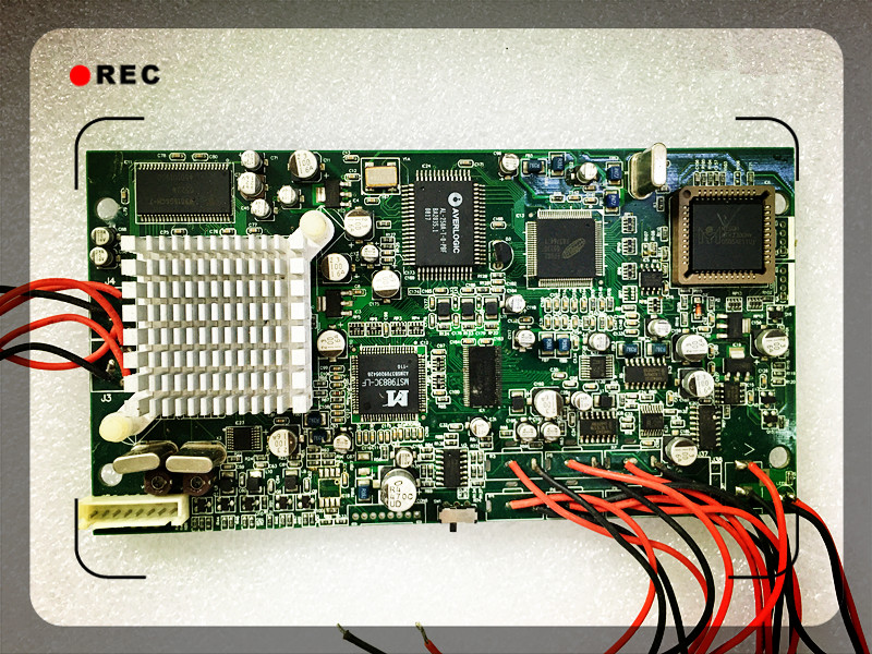
Grande PCBA Capability
1. The largest board: 310mm*410mm (SMT);
2. Maximum board thickness: 3mm;
3. Minimum board thickness: 0.5mm;
4. The smallest Chip component: 0201 package or components over 0.6mm*0.3mm;
5. The maximum weight of the mounted components: 150 grams;
6. Maximum component height: 25mm;
7. The largest component size: 150mm*150mm;
8. Minimum lead component spacing: 0.3mm;
9. The smallest spherical component (BGA) spacing: 0.3mm;
10. The smallest spherical component (BGA) diameter: 0.3mm;
11. Maximum component placement accuracy (100QFP): 25um@IPC;
12. Mounting capacity: 3-4 million points/day