
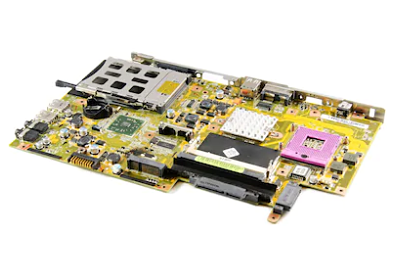
Once finished PCB design, checking the functions of all items is vital and indispensable. Just like when we finish the examination papers, we should do a simple analysis and check all the questions again to ensure that we do not make major mistakes due to negligence. Likewise, so does PCB design.

The following inspection items that need to be performed after PCB design:
1. DFM inspection of bare PCB board: Does the production of bare PCB board meet the technical requirements in PCB manufacturing? Including trace width, gap, trace, layout, vias, marking, wave soldering component direction, etc.
2. The consistency between actual components and pads: Does actual SMT components purchased are consistent with the design pads? ( If not, mark it with a red label) Does they meet the gap requirements of SMT Machine?
3. To generate three-dimensional (3D) graphics: Will spatial elements interfere with each other? Does layout look reasonable? Is it good for heat dissipation and SMT reflow soldering?
4. PCBA production line optimization: To optimize the loading sequence and soldering location of components. Input the existing pasting machine (such as Siemens high-speed machine, general multi-function machine) into the software, and assign the components to be pasted to the existing board. By considering how many types components pastes by Siemens, how many types of Siemens pastes, how many pasting methods Siemens have , How many pasting methods there are in the world, how many locations and where to pick up materials, etc. This is obviously able to optimize SMT chip processing program and save time. In addition, for multi-line pcba production, the distribution of solded components can also be optimized;
5. Operating instructions: To generate operating instructions for workers on the production line automatically;
6. Revision of inspection rules: Inspection rules can also be modified. For example, if the component gap is 0.1mm, circuit board complexity that can be setted as 0.2mm according to the specific model; If The trace width is 6mi, which can be changed to 5mil in high-density design;
7. Support Panasonic, Fuji, Universal patch software: Then it can automatically generate paste software and save a great number of programming time;
8. Generating steel plate optimization graphics automatically;
9. Generate AOI and X-ray programs automatically;
10. Checking whether support multiple software formats or not, such as Japan & USA’s KATENCE, China’s software PROTEL);
11. Checking BOM and mending related errors, such as spelling errors about manufacturer name; To convert BOM to software format.
PCB Design Ability
>The highest signal design rate: 10Gbps CML differential signal;
>The highest PCB design layers: 40 layers;
>Minimum trace width: 2.4mil;
>Minimum trace gap: 2.4mil;
>Minimum BGA PIN gap: 0.4mm;
>Minimum mechanical hole diameter: 6mil;
>Minimum laser drilling diameter: 4mil;
>Maximum PIN number:; 63000+
>Maximum number of components: 3600;
>Maximum number of BGA: 48+.
PCB Design Service Process
1. The customer provides Schematics to inquiry PCB design;
2. Evaluate the price according to the Schematics and customer’s design requirements;
3. The customer confirms the Quotation, signs the contract and arranges the project deposit;
4. Receive advance payment and arrange engineer to layout;
5. Finish PCB Layout, provide a screenshot of layout file to the customer for confirmation;
6. The customer confirms OK, settles the balance, and send PCB layout file to the customer.


