
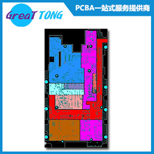
PCB Layout is based on the signal connections and signal features of schematic as well as the features of functional modules.
High-quality and Low-cost
PCB Manufacturing Services
![]() 1 to 30 Layers
1 to 30 Layers ![]() 100% Electrical Testing
100% Electrical Testing
![]() FR-4/Rogers/Teflon
FR-4/Rogers/Teflon ![]() Controlled Impedance
Controlled Impedance
Technical ArticleWhat is the difference between a schematic diagram and a PCB layout?Time:2018-12-14 17:32:14 Click:
PCB Layout is based on the signal connections and signal features of schematic as well as the features of functional modules.
Related articles:
Previous:How is the voltmeter and ammeter connected in a circuit? Next:What is the RO4350 PCB substrate made of? |
NewsOur Facilities |


