
What is the IMC layer?
The IMC layer is the inevitable part of PCBA soldering and the most vulnerable part of solder bonding.
Generally speaking, a good PCBA solder is formed, and the most vulnerable part of the solder bonding force is the IMC (Inter-Metallic Compound) layer. The IMC layer is a metal compound, and the IMC is more indispensable for good soldering. Shenzhen Grande described the IMC layer as a child who was extended after the combination of men and women. Here you can imagine this layer of IMC as a cement between bricks and bricks. It serves the purpose of joining two different bricks. The same is true for IMC. Without this layer of IMC, it is impossible to form a good weld between two different metals. However, this layer of IMC is also the most vulnerable part of the entire welded structure. Imagine that most of the brick walls will be impacted. The cement is cracked and the IMC layer is the same, so it is said that if the solder is affected by stress, it will usually be cracked first from the IMC layer.
How can we judge the IMC layer?
If the cement is not well coated or unevenly coated, some of it is painted, partially uncoated or the IMC layer is too thick or too thin. Does it affect the bonding force between the bricks? The answer is yes. If the part solder is found to be broken in the IMC layer, it is necessary to further analyze whether the IMC layer is good or not. The general judgment is to see if the IMC layer is continuous, evenly distributed, and usually use cross-section. And use a high power microscope to observe, and use EDX to view elemental analysis for further judgment.
What is the problem of IMC layer?
In general, if the surface of the PCB pad/pad or the soldering of the electronic component is oxidized, the IMC layer will not grow out or the IMC will not grow in some places. In addition, the reflow oven temperature may cause a similar phenomenon if the heating is insufficient.
As for the IMC layer which is too thick or too thin, although it will affect the solder bonding force, it has nothing to do with the SMT production process. The SMT process basically ensures that the IMC grows out and grows evenly. Mission, because the IMC layer will grow longer and thicker with time and heat accumulation. When the IMC grows too thick, the strength will become worse and become brittle. This is a bit like brick and brick. Like cement, the right amount of cement can bind different bricks tightly together, but if the cement is too thick, it is easy to be pushed down from the cement. This also explains why most products will be used for a long time. Getting worse.
Shenzhen Grande has been questioned since then, in the end, how thick is the IMC layer is the ideal thickness?Shenzhen Grande will use the current copper tin or copper nickel compound, the best thickness should be 1~3u", but the general thickness is only 1~5u" is acceptable.
Another factor that may occur in the SMT process and affect the solder strength is the presence of voids in the solder. These holes are due to the inability of the solder to escape the solder air or flux volatiles in the molten state, until the solder cools. It is formed by being wrapped in it, and there are two very obvious features for judging whether it is a wind hole:
1. The inner surface is smooth.
2. It has a round shape in the solder.
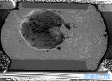
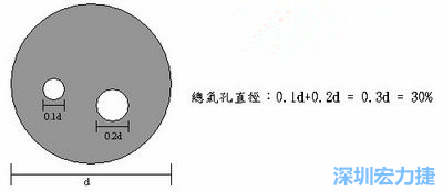
The larger the hole, the more unfavorable the soldering strength. How can the hollow lotus root be able to withstand folding, but the hole is difficult to avoid completely in the welding process, especially the BGA or QFN, LGA and other parts with a large amount of solder, which can specify holes at a certain ratio. Accepted, the technical progress has changed the specifications in the future. According to the requirements of IPC-7095B and IPC-A-610D, the total hole diameter of the BGA solder ball can not exceed 25% of the total diameter of the solder ball. Most electronics factories This is also used to determine the yield of the hole. If you have any changes in the future, please use the latest specifications.
BGA hole
BGA hole (void) size calculation
Therefore, it is only positively correlated with the quality or process of SMT when it is found that IMC does not come out or there is uneven distribution between the IMC and the interface. This correlation may be related to insufficient heat in the reflow oven, or it may be related to the poor surface finish of the PCB or the storage environment, or it may be related to the quality of the electronic parts. This requires more slicing and elemental analysis. Can judge.
Now you should be an expert. If you have a problem with solder rupture next time, please don't run to ask Shenzhen Grande right away. You can try to do some homework first.


