
Nowadays, PCB process has used CCL (copper clad laminate, copper foil substrates as standard materials. And each CCL factory will specify the peeling strength of its CCL copper foil in the product specifications it provides to its customers. From these specifications, we can clearly see that the peeling strength of using the thickness of 1.0oz copper foil is higher than that of using 0.5oz. Moreover, the peel strength of CCL is different among different models and manufacturers, so it is necessary to choose the CCL specification carefully to enhance the bonding force between copper foil and PCB sheet.
What is CCL (Copper Clad Laminate)?
With the evolution of technology and industrial division of labor, copper foil substrate (copper clad laminate, CCL) has become one of the standard raw materials for the (printed circuit board, PCB) manufacture of printed circuit boards. In the early days, the PCB plate factory also had to attach copper foil to the insulating substrate. It is no longer necessary now.
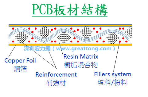
Today's PCB is basically composed of the following four materials:
Copper Foil
Reinforcement
Resin
Fillers
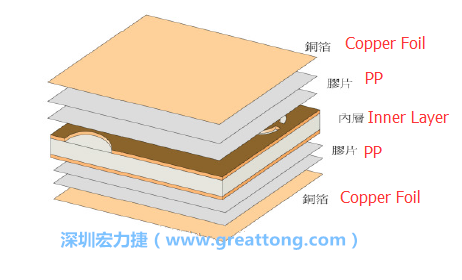
The copper foil is used as the power supply layer, the grounding layer and the electronic signal transfer layer, while the CCL is evenly coated with copper foil on the surface of a hard insulating substrate. The thickness of insulator and copper foil will be specified according to the needs of most customers, but it can also be added or decreased. According to the need of CCL, there can be single-sided copper foil and two-sided copper foil classification.
A modern PCB board factory basically chooses the required CCLs according to the Gerber files made by the customer, and then etches the line (trace), on the copper foil of the CCL and affix pp (prepreg, film to the adjacent CCL) to avoid the short circuit that should not occur between the different CCL copper foil layers. The PCB can be completed by connecting the interlayer line (similar to a building through a staircase) with a through hole (vias).
How about the classification of CCL?
CCL (copper foil substrate) generally has different grades and applications according to different substrate materials. The materials of PCB are respectively paper substrates, composite substrates and fr4 substrates, and their properties and uses are different.
"Paper Substrate" (FR-1MFR-2) is made of phenolic resin and Kraft paper, which is of low grade. Its biggest advantage is low cost and low price, but its structure strength is poor, and it can only be made into a single-layer printed circuit board. Paper substrates are used in a wide range of areas, but are mostly products with simple wiring and lower technical levels, such as remote controls, televisions, radios, computer keyboards. Such products, its internal use of printed circuit boards are mostly made of paper substrate.
"Composite substrate (cem series)" uses epoxy resin (epoxy) as raw material, reinforced fabric material is glass fiber cloth and Kraft paper or glass fiber paper, its strength is better than paper substrate, so it can carry higher weight. The composite substrates are used less because they are in awkward areas because of their durability and price, mainly used in video games and 17 "or more computer screens."
The "FR-4 Substrate" is currently the highest grade of copper foil substrates. The resin is epoxy resin, and the reinforced fabric is made of multi layer glass fiber cloth, (Glass Fiber, GF) compacted. Fr4 substrates are widely used in computer components, mobile phones, and peripheral equipment. For example, the printed circuit boards used in computer motherboards, hard disk machines, mobile phone motherboards and other products are all manufactured from FR4 substrates.
Note: FR is an acronym for [flame retardant (flame retardant] to indicate that the material conforms to the ul94v-0.FR-4 name originally created by nema in 1968.


