1. Schematics (Necessary)
Whether it is drawn by hand or drawn by CAD, in short, only got Schematics can start PCB Layout;
2. The circuit power consumption calculation sheet (Unnecessary)
There are data about the power supply voltage and the current flowing through every single component. Without this, you need to interpret the Schematics to design the trace width and trace spacing.
In the absence of special software, free software such as LTspice can be used for circuit simulation.
In addition, verify through written calculations, and record the voltage value, positive and negative, current value and direction of flow for the places you need to check in the future.
The application in circuit board design is to calculate the width of the trace based on the current flowing through a certain area, especially for voltage traces and GND traces so that it can be used as a basis for designing connections the size and number of holes.
3. The electrical list of the Schematics (Unnecessary)
If no electrical list of the Schematics, which is able to make by yourself in the light of the Schematics. After all, the circuit electrical list is necessary for circuit board design.
Bt the way, the electrical network list for the circuit board is divided into a circuit diagram electrical network list and a circuit board electrical network list.
In many cases, especially when the circuit board is revised, the electrical network list will not be given. At this time, you need to do it yourself.
4. Bill of Materials (BOM) (Necessary)
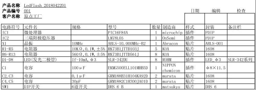
Here to compare the consistency of the Schematics and the BOM. And mainly two reasons causing the inconsistency:
1>Constant changing when designing new products;
2>Components are eliminated or updated when the product is revised;
Therefore, no matter how much time it takes, the Schematics must be consistent with the component list to ensure the success rate of the PCB Layout.
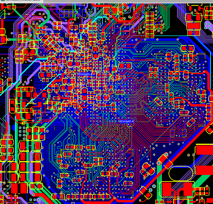
5. Circuit board design drawings (Necessary)
Even scribbled handwriting is still terribly necessary. If it is only delivered verbally, which will be possible lead to errors due to misunderstand the meaning of the product designer.
The content of the drawing: Board, surface treatment, the minimum limit of trace width and trace spacing, the specifications of the pads, the font and size of the printing.
The size of the circuit board, the location where the specified component is placed, and the prohibited area. Insulation specifications between different areas, etc.
6. Circuit board layout schedule
Calculate how long the circuit board layout takes, and how many layout engineers requries.
7. Circuit board area estimation table
Within the specified circuit board size, judge whether the components can be reasonably arranged in the circuit board.
In the case that the components can be arranged in the circuit board, it is judged whether to adopt a two-layer design, four-layer design or more.
Apart from that, in the absence of any designation, it is also necessary to fully communicate with the product designer to recommend the most appropriate circuit board size and layer design.
8. Workpiece size estimation table
After determining the size of the circuit board, in order to achieve the minimum production cost in production, several individual circuit boards will be connected together by V-cutting. At this time, the appropriate workpiece size must be selected.
9. Circuit board electrical design table
It includes the following parts:
1>Trace width calculation table or trace width reference table;
2>Trace spacing calculation table or trace spacing reference table;
3>Connection hole pads size calculation table or Connection hole pads size reference table.