
Visual inspection is a process that must be carried out after PCB Assembly. As you probably know, visual inspection is mainly for the appearance of PCB components and solder joints, and which is also a timely feedback to PCB Assembly as well as improve the soldering of SMT Assembly and product quality.
>Basic working conditions for visual inspection
1. Working conditions: Temperature [ 18°C to 28°C], Humidity [35%~75%];
2. Operation object: All assembled PCB boards;
3. Operator: With certain general SMT and DIP welding status discrimination ability;
4. Job responsibilities: Compare and screen bad welds, write down bad marks, and fill in the corresponding forms.

> Materials required for visual inspection
1. PCBA: Quantity;
2. Label and record of bad product: 1 copy;
3. Anti-static wrist: 1;
4. Anti-static gloves: 1 pair;
5. Anti-static rotating jig: Several.
>Visual inspection procedure
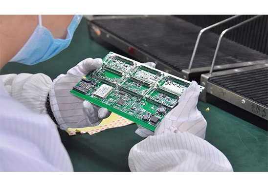
1. Wear anti-static clothes, anti-static wrists and gloves then sit down;
2. Paste the PCBA serial numbers to follow-up quality tracking.
3. Hold the PCBA with both hands and keep the tilt angle of 45°. From left to right, scan key components and connectors line by line from top to bottom to see if there is any bad soldering.
4. Take the long side of the PCBA as the axis and rotate at will at a certain angle to observe whether the key components have bad angles of buoyancy, skew, missing welding and missing welding.
5. If a poorly welded component or connector is found and cannot be determined by itself, the on-site management should be consulted to confirm whether it is qualified, and no judgment should be made at will.
6. When the defective product is found to be obviously defective, the label of the defective product is only the label. Please note that the label of the defective product points to the defective arrow.
7. Flip to the other side of the PCBA and focus on the soldering quality of the connector solder joints: whether there is even tin, missing solder, little solder joints, cold soldering, tin tip, dirt, etc., and abnormal adhesion is found The defective label is distinguished and placed on the shelf of the defective product.
8. Visually inspect key components several times and place abnormal products on the shelf of qualified products.
9. Every 10 PCBA boards should be carried out in groups, and the relevant records should be verified for completeness and transferred to the next process if there is no omission.
10. Fill in the bad product record list, and fill in the description of the bad phenomenon according to the serial number.
11. Defective products should be placed in the specified relatively fixed position, and clearly marked, not to be confused.


