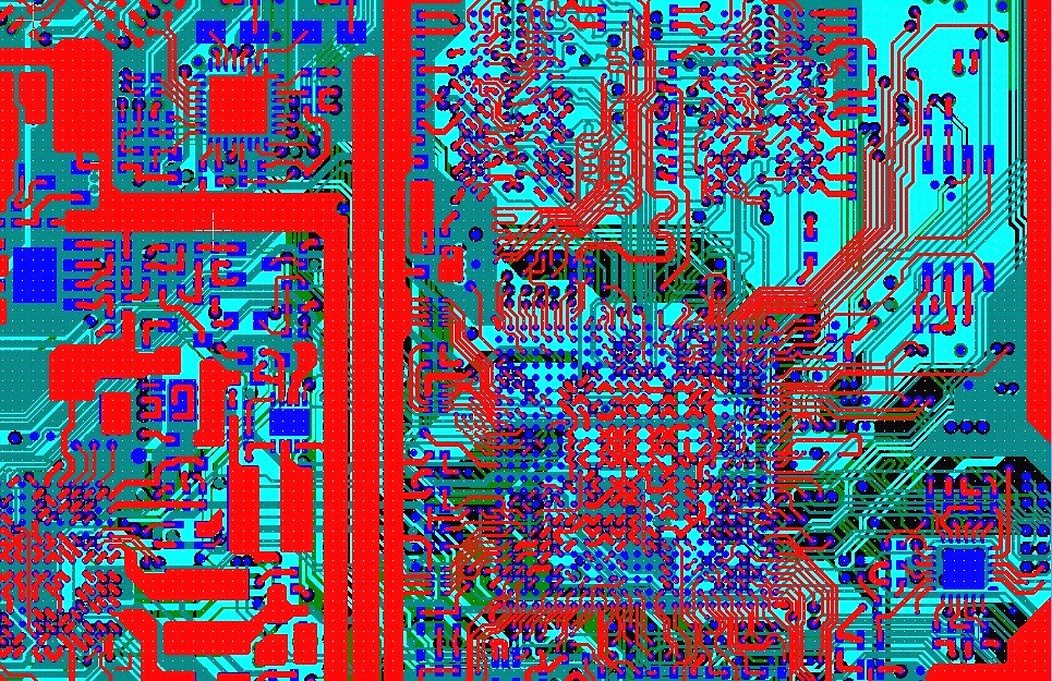
Multi layer PCBs are beneficial to products because they can handle greater complexity. Computers, telephones, and medical equipment are some examples of applications that benefit from multilayer PCB layout. However, the use of multilayer printed circuit boards will connect these layers to each other as a key issue. If you don't connect each layer to the corresponding point, you will end up gluing multiple single-layer printed circuit boards together.
Input Via
It is one of the smart solutions to connect each layer vertically. However, Vias need to understand the annular ring to work properly. These rings are defined as the minimum distance between the drilled hole and the edge of the via trace. The larger the annular ring, the larger the copper connection around the borehole.
The use of an annular ring usually determines the size of the shot. Do you use Altium component placement when soldering to one or both sides of the circuit board? And considering soldering, you may need a larger area. Are you just using this channel as a test point without soldering? The smaller ring size can help you.
No matter what application you use toroids in your circuit board layout, you can easily determine the size by referring to our trusted old friend IPC-7251. This document recommends a ring width of 250μm to obtain the maximum material condition (MMC). MMC just means you will have the most powerful solder joints. On the other hand, 150μm is the recommended width of the annular ring to achieve the minimum material condition (LMC). LMC simply means that you will use the most unstable solder joint to connect away.
Obviously, these are just suggestions and should be changed in the light of your specific application.
Manufacturing Tolerances Of Multilayer PCB Layout
When any combination of multiple manufacturing processes occurs in a production environment, there will usually be slight overlap errors due to incomplete tolerances here and there. Specifically, when you etch copper traces on the printed circuit board and during the process of drilling through the traces, your drilling will usually not be completely aligned with the center of these traces and will make you slightly Deviate. But don't be afraid, the tolerance is here!
Since you should have PCB layout and manufacturing tolerance errors, PCB layout ring tolerance errors are no exception. First, by determining manufacturer-specific tolerances, they will be able to accommodate errors, and by determining the minimum width of the annular ring that can be safe, you can reduce the risk of the entire manufacturing process and ensure that the minimum is always reached.
In short, know that there will be some manufacturing errors in this process, but the above-mentioned errors in PCB design will make you higher than the minimum, especially the annular ring with drilled through holes.
Drilling tolerance plays an important role in determining the size of the annular ring.
Calculate The Annular Ring Width
An easy way to verify that the width is suitable for printed circuit board (PCB) layout is to calculate the maximum width to run after production. The following equation can be used:
((Diameter of trace pad)-(Diameter of drill hole))/2=(Maximum annular ring width)
The larger the tolerance, the smaller the manufacturing error and the smaller the annular ring width. The larger the hole diameter, the smaller the width of the annular ring.
Know that the width of the annular ring should be able to provide a strong enough connection for electrical and mechanical connections, and be able to recognize that manufacturing tolerances will keep your annular ring width at an acceptable distance, and do not even touch the trace pad when drilling Next.
When the via is designed by the PCB to the micro area, you will need PCB design software, which can fully specify the annular ring width and the manufacturing tolerance of the via. Fortunately, Altium Designer can easily handle sensitive circuit board layout complexity through a complete PCB design rule check list and intuitive circuit board layout software.