Grande is a PCB manufacturer with more than 20 years of experience in PCB & PCBA manufacturing whom specializes in PCB prototype of impedance board, HDI board and other multilayer PCB as well as small and medium volume production.
As we all know, there are simple and complex PCB boards. Simple PCB boards are easy to prototype; However, if it is a complex circuit board(PCB) prototype, then we must pay attention to. In other words, if we don’t make full use of the relevant inspection tools during the PCB prototype process, in case something goes wrong, which would be too late until the PCB board was ready. Therefore, we must make full preparations before prototype.
Preparation Before PCB Prototype
1. Making The Physical Frame
The closed physical frame is like a basic platform for the coming component layout and PCB prototype. Accuracy is deserve to concerns a lot. Furthermore, it is best to use arcs at the corners, which can not only avoid scratches by sharp corners, but also reduce stress.
2. Inporting Components & Networks; And Layout For Components
When layout components and networks into the frame of PCB prototype, you must carefully follow the prompts, including the packaging form of the components and the problem of the component network. Because of the contrast prompts, problems are not easy to occur. Layout components and traces have a great impact on product life, stability, and electromagnetic compatibility during PCB proofing, so special attention should be paid. Generally speaking, there should be the following principles: placing order and paying attention to heat dissipation.
3. PCB Layout & Adjustment
It is best to pay attention to the requirements of processing parameters when layout and routing PCB, or place the order to a reliable PCB prototype manufacturer, the defective rate will be greatly reduced. After completing the PCB layout and routing, all you need to do is to adjust the text, individual components, routing and apply copper (this work should not be too early, otherwise it will affect the speed and bring troubles to the PCB design and wiring), the same is for It is convenient for production, debugging and PCB layout and routing;
4. Checking The Network
Sometimes the network relationship of the PCB board drawn is different from the schematic diagram due to misoperation or negligence. At this time, inspection and verification are necessary. So after finishing painting, you should check it first, and then do follow-up work.
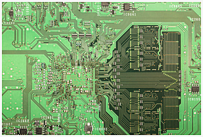
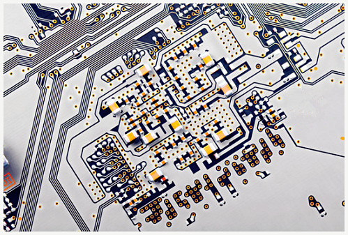
PCB Prototype
Grande PCB Prototype advantages
Mass production: 2- 14 layers;
Small & Medium Production: 14-22 layers
Minimum Ttrace width/spacing: 3mil/3mil
BGA spacing: 0.20MM
Smallest Aperture of finished PCB: 0.1mm
Size: 610mmX1200mm
Solder Mask: Japanese Tamura, Taiyo, Fu Duo Ken;
FR4: Shengyi, Kingboard, Haigang, Hongren, Guoji, Hazheng, Nanya,
(Shengyi S1130/S1141/S1170), Tg130℃/ Tg170℃ Tg180℃ Contour TG sheet)
High Frequency Board: Rogers (Rogers), Taconic, ARLLON;
Surface Technology: spray tin, lead-free spray tin, full board gold plating, plug gold plating, full board thick gold, chemical tin (silver), anti-oxidation (OSP) blue glue, carbon oil
The above mentioned meshod work that should be prepared before PCB prtotype. In addition, when choosing a prototype company, the best choice is a PCB proofing company with a good reputation, so as to improve the accuracy of the PCB board.