Welcome to Grande (Shenzhen) Electronic Co., Ltd.!
High-quality and Low-cost
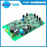
PCB Manufacturing Services
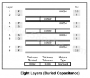
![]() 1 to 30 Layers
1 to 30 Layers ![]() 100% Electrical Testing
100% Electrical Testing
![]() FR-4/Rogers/Teflon
FR-4/Rogers/Teflon ![]() Controlled Impedance
Controlled Impedance
2018-08-08
2018-05-21
2017-12-25
2017-12-23
2017-12-21
2017-12-20
2017-12-04

2017-11-23
2017-10-19
2017-10-17
