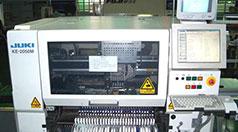
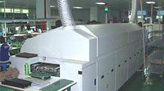
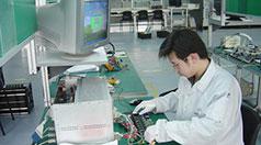
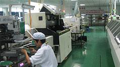
Designing a printed circuit board is a long process; determining your performance specifications, researching components, pouring over datasheets to be sure they will fit your needs, and simulating your design. Once you’re satisfied with your design the last stage is production.
We at Shenzhen Grande Electronics do our best to make this as stress free as possible with our turnkey PCB Assembly service. Just send us your design (in Gerber & centroid or ODB++) and Bill of Materials (BOM) and we will fabricate the board, order the parts and assemble. This way you do not need to source the parts yourself and deal with a separate manufacturer and assembler. To make this process even easier for you, here are some tips to check your design to avoid some common delays.
1. Do your Gerber Files load correctly?
If you are new to exporting your circuit designs for manufacturing, it is recommended that you double check the gerber files exported from your design program in a separate gerber file viewer. Shenzhen Grande recommends the ViewMate free gerber viewer. Things to look for in your files include: do the files load in the viewer, are the trace widths as you intended, are the layers aligned, and any other variations from your design.
2. Do your traces meet your manufacturer’s requirements?
We at Shenzhen Grande can manufacture a minimum trace width of 4 mils and a minimum trace spacing of 3 mils. These values increase with higher copper weights. You can double check these measurements in your gerber file viewer.
3. Do you have a layer for your board outline and are your components far enough from the board edge?
We at Shenzhen Grande require a clearance of all components and traces to the board edge of 8 mils but for connectors or gold fingers required to be at the board’s edge please contact us to see if we can meet your needs. The benefit of the board outline layer is we are able to cut boards with any outline shape.
4. Did you include a centroid file for pick and place?
For automated assembly, a file is needed to instruct the machine where each component should be placed and in what orientation. More info on this file here. ODB++ includes this file automatically, but gerber files require this to be submitted separately.
5. Are your chosen parts available for order?
One of the most common delays in assembled PCB manufacturing is part availability. You can avoid this issue by checking your BOM availability using an online service such as Octopart and FindChips. Availability does fluctuate so do this right before you RFQ or place an order. If you have a specialty part in your design that is not available at popular distributors you may wish to purchase this part yourself and consign it for assembly.
6. Did you include a drill file?
A drill file specifies the location and size of holes drilled into your board. Some CAD software may require a separate step or option to export a drill file when generating gerber files. Double check that your drill file is included before submitting.
Welcome to Shenzhen Grande Electronic Co., Ltd.!


