HDI stands for High Density Interconnector. A circuit board which has a higher wiring density per unit area as opposed to conventional board is called as HDI PCB. HDI PCBs have finer spaces and lines, minor vias and capture pads and higher connection pad density. It is helpful in enhancing electrical performance and reduction in weight and size of the equipment. HDI PCB is the better option for high-layer count and costly laminated boards.
Regarding the electrical needs of high-speed signal, the board should have various features i.e. high-frequency transmission capability, impedance control, decreases redundant radiation, etc. The board should be enhanced in the density because of the miniaturization and arrays of the electronic parts. In addition, to the result of the assembling techniques of leadless, fine pitch package and direct chip bonding, the board is even featured with exceptional high-density.
Innumerable benefits are associated with HDI PCB, like high speed, small size and high frequency. It is the primary part of portable computers, personal computers, and mobile phones. Currently, HDI PCB is extensively used in other end user products i.e. as MP3 players and game consoles, etc.
HDI PCBs take advantage of the most recent technologies existing to amplify the functionality of circuit boards by means of the similar or little amounts of area. This development in board technology is motivated by the tininess of parts and semiconductor packages that assist superior characteristics in innovative new products like touch screen tabs.
HDI PCBs are described by high-density features comprising of laser micro-vias, high performance thin materials and fine lines. The better density allows extra functions per unit area. These types of multifaceted structures give the required routing resolution for large pin-count chips which are used in mobile devices and other high technology products.
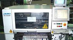
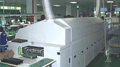
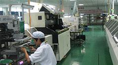
The placement of the parts on the circuit board needs extra precision than conservative board design due to miniature pads and fine pitch of the circuitry on the circuit board. Leadless chips require special soldering methods and additional steps in the assembly and repair process.
The lesser weight and size of the HDI circuitry means the PCBs fit into the little spaces and have a smaller amount of mass than conservative PCB designs. The smaller weight and size even signifies that there is lesser chance of harm from mechanical shocks.
Welcome to Shenzhen Grande Electronic Co., Ltd.!


