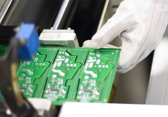
In order to meet customer requirements, the printed circuit board (PCB) via hole must be plugged. After a host of practice, the traditional aluminum plugging process is changed, and the circuit board surface solder mask and plugging are completed with white mesh. Production stable and quality reliable.
As you probably know, via hole plays the role of interconnection and conduction of traces. The development of the electronics industry not only promotes the development of PCB, but also puts forward higher requirements on PCB manufacturing technology and SMT Assembly technology. Via hole plugging technology came into being, and should meet the following requirements:
1. There is copper in the via hole, and the solder mask can be plugged or not plugged;
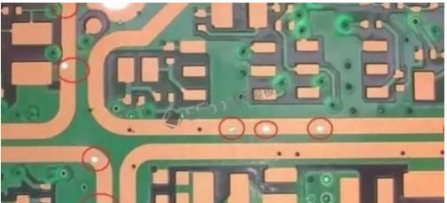
2. There must be tin and lead in the via hole, with a certain thickness requirement (4 microns), and no solder mask should enter the hole, causing tin beads in the hole;
3. The through holes must have solder mask plug holes, opaque, and must not have tin rings, tin beads, and flatness requirements.
With the development of electronic products in the direction of "light, thin, short and small", PCBs have also developed to high density and high difficulty. Therefore, a large number of SMT and BGA PCBs have appeared, and customers require plugging when mounting components, mainly five functions:
1. Prevent the tin from passing through the component surface through the via hole to cause short circuit when the PCB is wave soldered; Especially when we put the via on the BGA pad, we must first plug the hole and then plate it with gold to facilitate the BGA soldering.
2. Avoid flux residue in the vias;
3. After the electronics factory SMT Assembly are completed, the PCB must be vacuumed on the testing machine to form a negative pressure before it is completed:
4. Prevent surface solder paste from flowing into the hole, causing false soldering and affecting placement;
5. Prevent the tin balls from popping up during wave soldering, causing short circuits.
Grande PCB Manufacturing Advantages
1. Energy production from 2 to 14 layers, 14-22 layers can be sampled and produced.
2. Minimum trace width/spacing: 3mil/3mil BGA spacing: 0.20MM
3. The minimum aperture of the finished product: 0.1mm Size: 610mmX1200mm
4. Solder Mask Material Brand: Japanese Tamura, Taiyo, Fudokan;
5. FR4: Shengyi, Kingboard, Haigang, Hongren, Guoji, Hazheng, Nanya,
(Shengyi S1130/S1141/S1170), Tg130℃/ Tg170℃ Tg180℃ Contour TG sheet)
6. High frequency board: Rogers (Rogers), Taconic, ARLLON;
7. Surface technology: spray tin, lead-free tin spray, immersion gold (ENIG), full board gold plating, plug gold plating, full board thick gold, chemical tin (silver), anti-oxidation (OSP) blue glue, carbon oil.